Testing of Printed Transwells for SEPCON chips

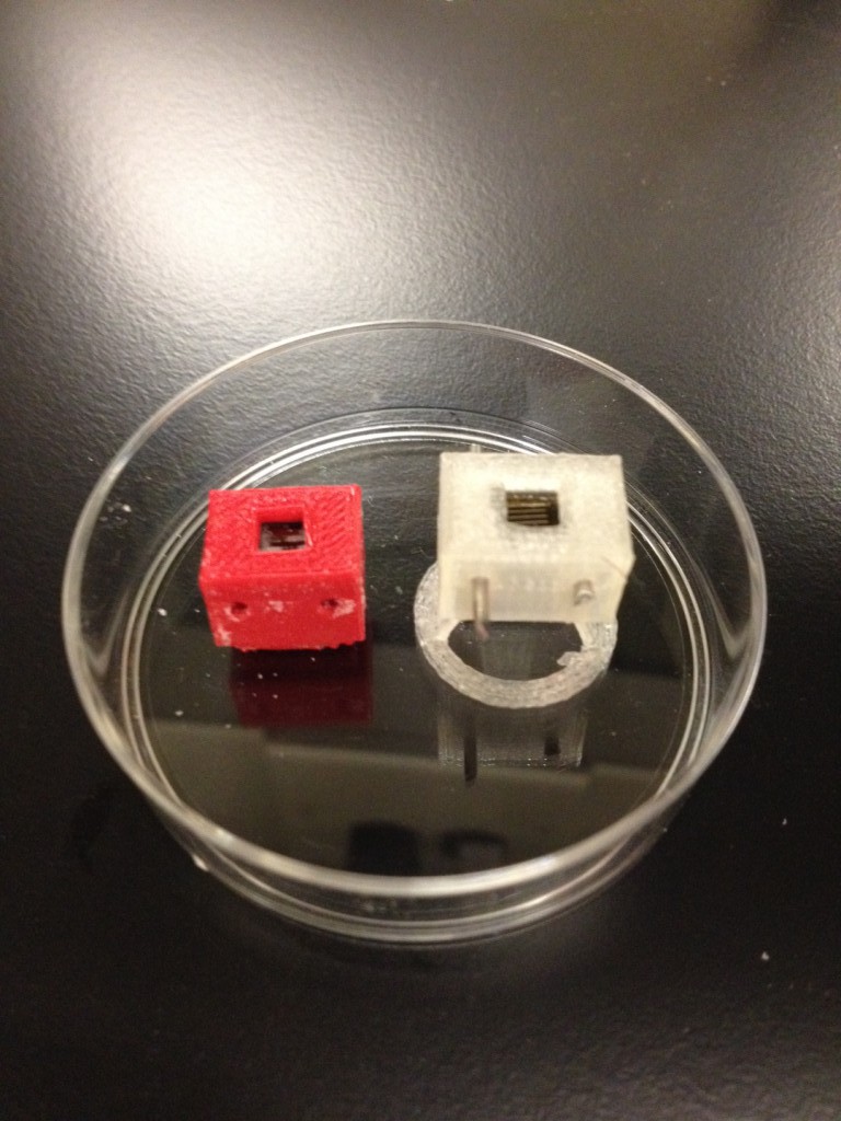
Testing was performed on 3D-printed transwell device prototypes for use as culture devices with SEPCON chip integration(Makerbot2 printed Transwells for SEPCON chips). The performed testing attempted to determine the quality of seal of interfaces between all device components. The two devices tested were identical in basket geometry, with the only differences being in printing material. One was composed of natural PLA, the other composed of dyed PLA (see Figure 1). Both were printed with the improved fabrication specification of 100% infill.
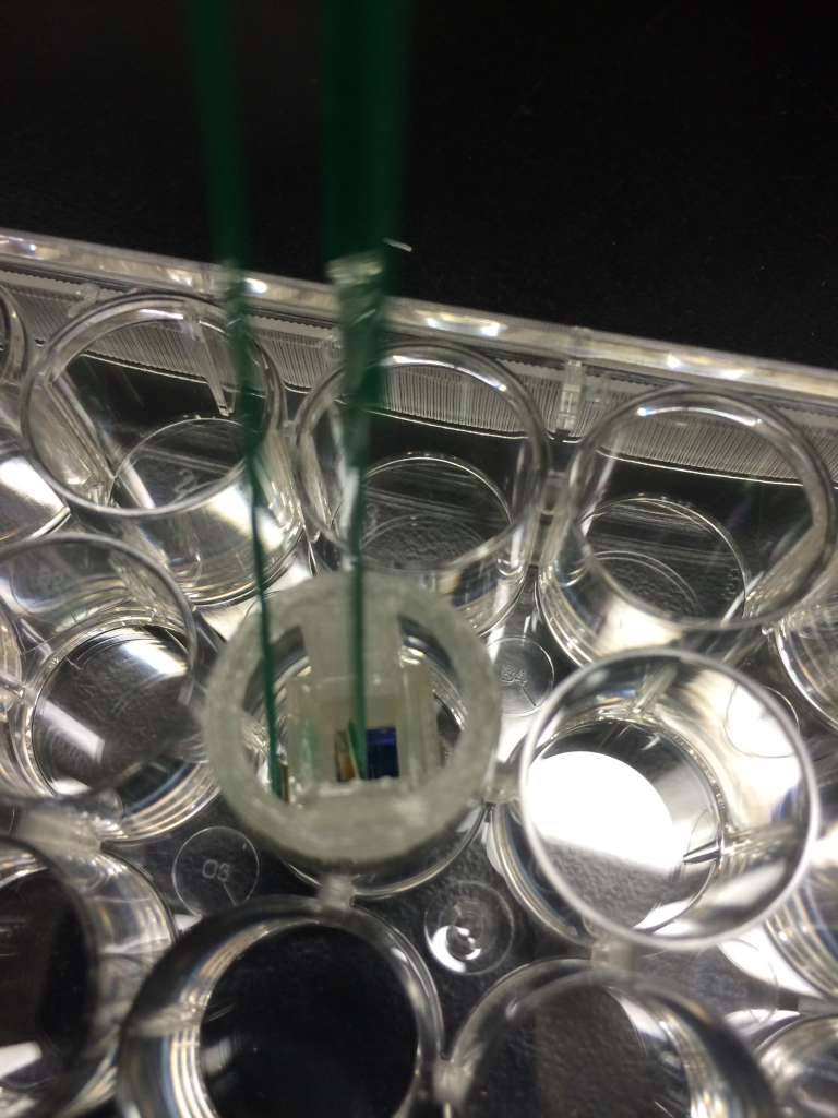
Both devices displayed adequate seal through dye testing. TEER measurements were performed with an EVOM2 epithelial voltohmeter and a set of chopstick electrodes to determine the impedance across the device as an indication of seal quality (see Figure 2). A reading indicating an open circuit would indicate no interaction between the solution in the transwell chamber and the bulk solution, a perfect seal. For the purposes of our measurement, an impedance close to the maximum measurement capability of the EVOM2 at 12k is sufficient to indicate a seal. A short circuit indicates interaction of solutions that are separated by the chip. This reading should be as close to 0 as possible.
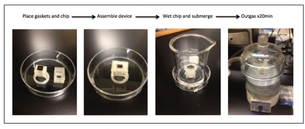
Each device was carefully assembled, with SEPCON chips positioned between two square gaskets and PLA basket components. The basket was pinned in place. Following various measurements where air bubble were introduced into the trench-side chamber of the device, the protocol for device preparation was improved to include wetting on both sides of the chip, immersion in PBS, then outgassing to remove any air bubbles that might affect the resistance reading (see Figure 3).
The resistance of the bulk PBS solution was measured prior to each resistance measurement, via immersion of both electrodes in the bulk solution, to ensure a short circuit. Resistance across the device was measured by positioning chopsticks such that one electrode was in the bulk and one was within the transwell chamber (see Figure 2).
Device testing was performed with the integration of a non-porous (0% porosity), 1060 chip, and later a chip with 10% porosity (number). An effective open-circuit measurement was sought, to serve as an indication of isolation of the transwell chamber from the bulk, verifying no leakage at component interfaces.
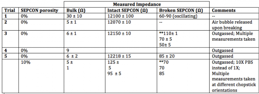
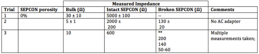
From these preliminary design tests on the devices, we determined that the RED PLA, although expected to have adequate sealance due to preferential printing properties when compared to that of the Natural PLA, did not have an adequate seal, as indicated by the repeated measurement of a low impedance, under what should have been open-circuit conditions (0% porosity). Thus, any TEER measurement with a permeable membrane would not be measuring the impedance due to the permeability of the membrane. We did not perform further testing with a permeable SEPCON with the red PLA for this reason.
Under all conditions, the natural PLA had an impedance measurement around the maximum measurement capability of the EVOM2 device. An open circuit is thus created across the SEPCON between the transwell chamber and the bulk. The seal is adequate. All fracturing of membranes, further, resulted a severe drop in impedance, indicating a short circuit configuration due to the solution interaction enabled by the fracture of the 0% membrane. Upon testing the 10% SEPCON configuration, impedance was severely decreased due to the porosity, as predicted.
Throughout the course of data collection, protocols were adjusted, and considerations for improvements were made. The addition of a wetting and outgassing step following device assembly is noteworthy in that it reduced the presence of bubbles at the chip surface that might alter impedance measurements. However, upon viewing trial devices under light microscope, we saw the repeated appearance of a bubble after wetting in the same corner, suggesting a small flaw in the printing of the device, such as a stray particulate (see Figure 4).

There was difficulty in the placement of the gaskets and chips on the surface of the PLA that may be approved by a slight trench of device- gasket interface, with slightly thicker gaskets.
Further, the measurement device was utilized with the AC adapter, causing a potential non-isolated measurement set up, and any movement of the chopsticks could result in a slightly different impedance reading. Hopefully, the battery pack replacement that has been ordered will correct, or at least minimize these issues.
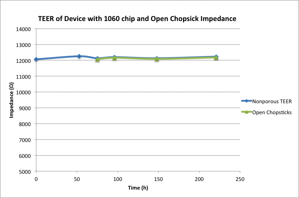
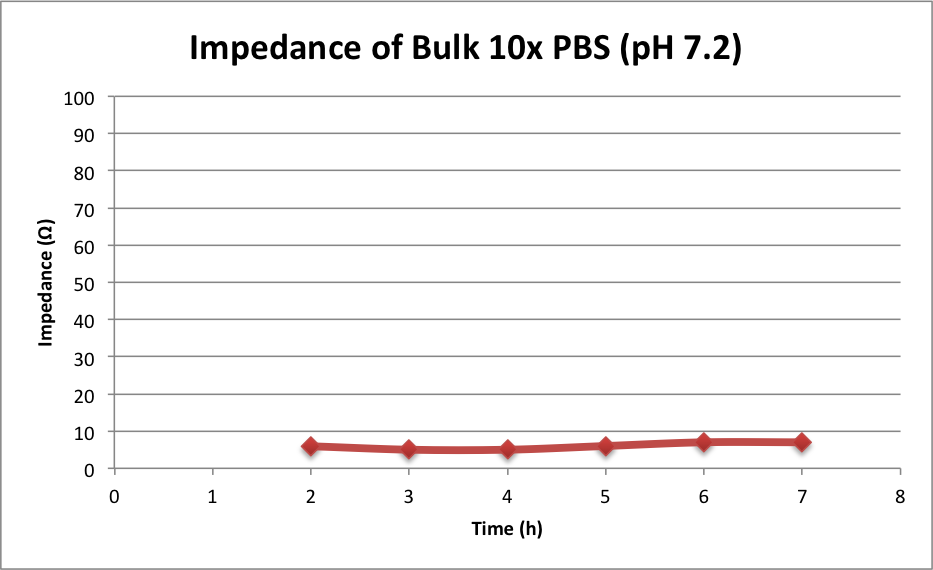
We then tested the device for a sustained seal over a week period. The device maintained seal over this period (see Figure 5,6).
Finalized Assembly Protocol (f0r now):
(1) Place gasket on chambered insert
(2) Place SEPCON square on gasket
(3) Place gasket on basket components
(4) Invert basket, slide onto insert
(5) Pin basket & insert together
(6) Whet surface on both sides of chip
(7) Place abridged over two gaskets in beaker with 10 mL PBS
(8) Outgas x20min
(9) Inspect for bubbles
Design considerations:
(1) Gasket considerations
(2) Wider tolerance on insert
(3)6-well plate design
Finalized measurement protocol (f0r now):
(1) Calibrate EVOM2 — 1000 Ohms
(2)Rinse chopstick electrodes in PBS
(3) Measure resistance of Rinse PBS to ensure short (nearly 0 impedance)
(4)Measure resistance of bulk (following bubble removal and inspection), should have nearly 0 impedance
(5) Measure TEER resistance across transwell membrane with consistent chopstick orientation
Measurement considerations:
(1) Complete removal of bubbles
(2) Replace battery pack to measure without AC adapter (causes non-isolated measurements)
(3) Consistent bulk solution (1X or 10X PBS)
(4) Chopstick orientation convention (dynamic position of electrodes can swing measurements by as much as 20 Ohms)
Very nice work. Although the inability to use cool colors could really slow down adoption. Looking forward to the follow ups to eliminate bubbles and improve stability.
I would also point out that the trials did not proceed as numbered (1-5). We did a few nonporous measurements, then switched to the porous membrane, and then switched back to the nonporous membrane, showing that we did not compromise the device’s sealing when we repeatably removed and reinserted chips.
Wow guys! This is great stuff – absolutely can’t wait to try these with cells!