Successful SiO2 Membrane Liftoff
Bob and I have been busy for the last couple of weeks going through the fabrication process with the hopes of SiO2 membrane liftoff. The fabrication process was similar to the silicon nitride membrane liftoff. The process is shown in the figure below.
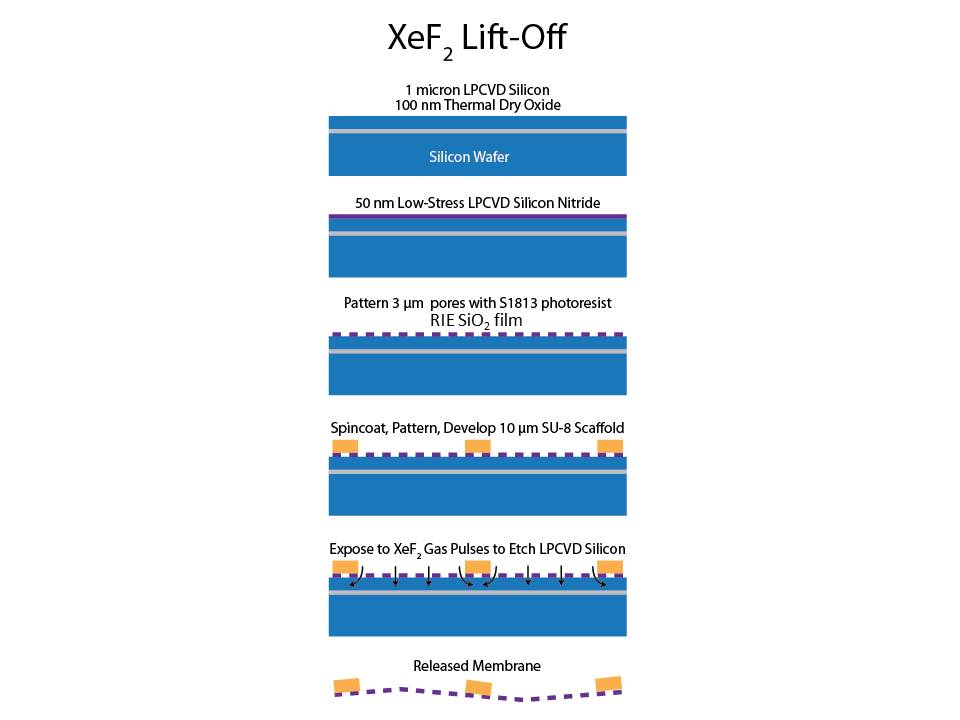
In the beginning, we started with 9 wafers that had thermal oxide grown (~100nm) on them. The thermal oxide acted as a etch stop. Then, the polysilicon was deposited onto the wafers using the LPCVD. The thickness of the polysilicon for four wafers was 127 nm and the rest of the wafers had 1080 nm. Down the line, we want to investigate if having a thinner layer of polysilicon will reduce the liftoff time without sacrificing the overall membrane film stress. Looking back, a RCA clean should of taken place to remove the contaminants from the LPCVD.
The TEOS was then deposited onto the polysilicon. The thickness was 300 nm. The P500 broke down after the TEOS was deposited on the wafers with 1080 nm polysilicon. There was a two day delay period before the rest of the wafers had TEOS deposited. The wafers were then place into the Bruce furnace for 8 hours at 600 ˚C with forming gas (H2/N2). The film stress of the TEOS was measured to be 31.5 MPa, but it is not certain if this is correct. The annealing process could of affected the film stress of the polysilicon, which then would give us an inaccurate measurement of film stress if the baseline has changed.
After the annealing process, 3 micron pores were patterned and etched on two wafers (one of each kind). The resist was not thick enough for the RIE. It was visible that part of the TEOS layer was etched away. Right now it is unknown how much was etched away, but next time, a thicker resist will be used to prevent this. Su-8 was spinncoated onto the two patterned wafers and exposed with UV light for the grid scaffold. Small pieces (2cm by 2 cm) were cleaved from each wafers; center and edge, and placed into a 10:1 BOE bath with surfactant for 10 seconds to remove the native oxide. The BOE etched away some of the membrane but it is unknown how much. The pieces were then placed in the Xatic right away for liftoff. As the silicon was etched away, a visible color change could be seen. For the 1080 nm polysilicon, it took 14 pulses, while the the 127 nm polysilicon required 18 pulses, which was an overkill. The membranes were transfered to PDMS posts. Overall, the glass membranes are more fragile than the nitride membranes which made it difficult to handle.

