New Wafers
A few of the newest SC wafers came back with intact samples without any pinholes. First here is a list of the experiments that we want to do in our lab with intact/pinhole free membranes
1. Protein separations – Requires >10 samples per wafer (preferably even more) for replicates of separations in both pressure and diffusion
2. Nanoparticle separations – Initially I only need a handful of samples to see if this actually works. Later on more samples with different cutoffs will be necessary for a full study.
3. DNA – Bill Bernhard’s group is looking to separate a DNA ladder and will need a handful of samples now for preliminary tests. Eventually they will need their own entire wafer to perform their DNA strand break experiments.
4. Rhodamine Diffusion with RTP – Anant wants to see if RTP treatment changes pore sizes and will need a few samples without pinholes to study this.
5. Dye transfer through cell monolayers – Barrett will need samples soon (within a month) for diffusion tests. When this is underway, a large amount of membranes will be required.
If I’ve missed anything, please comment.
Protein separations are currently the most pressing experiments, although I can only run the experiments if I have enough samples on one wafer. Excess samples or samples from wafers that don’t have enough for separations will get rerouted to nanoparticles, DNA, and rhodamine diffusion.
I looked at the newest wafers and here’s what we have (SC 019,022,023 had no intact/ph free samples):
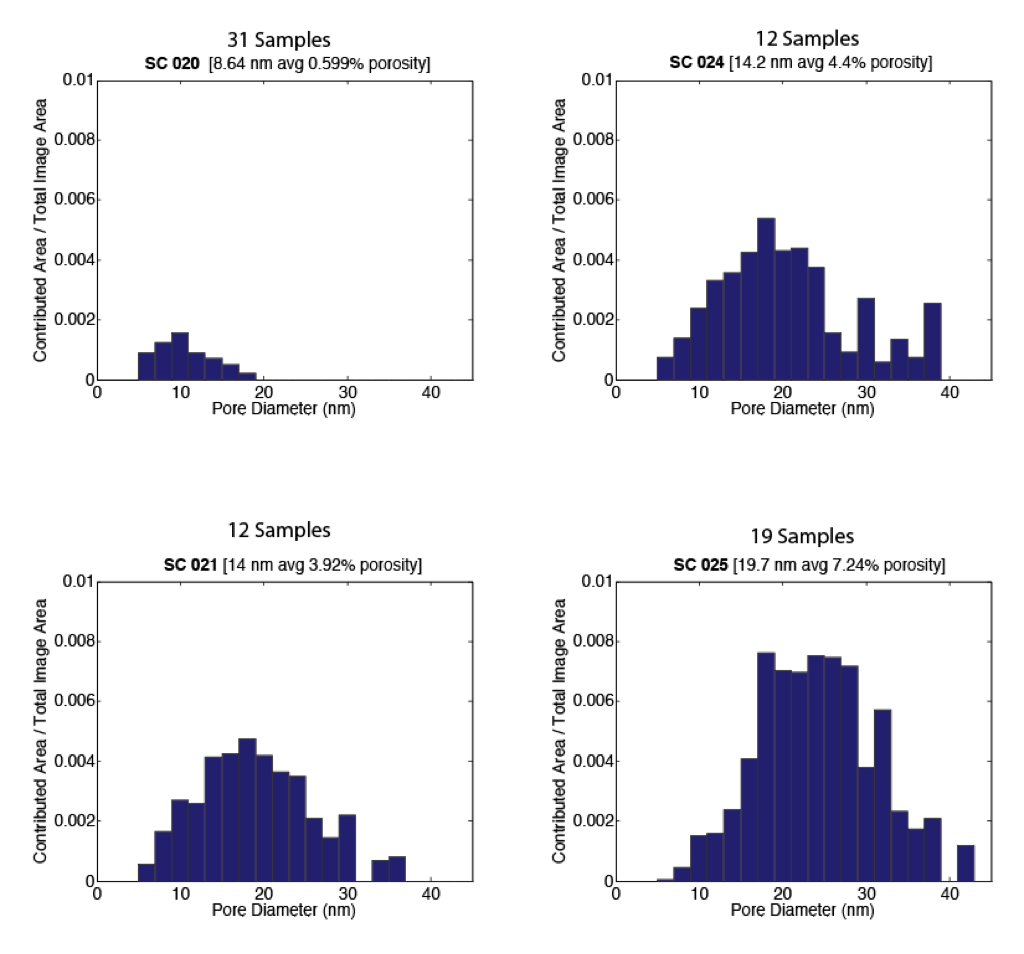
SC 020 is the wafer that’s not totally crystallized, and it has a low porosity with small pores. This wafer also has the most samples on it and may be good for separations (as long as we’re not concerned about the low porosity). Burst pressure may be barely high enough. Is there any reason that we would not want to use this unique, partially crystallized wafer for experiments?
SC 021, 024, and 025 have almost enough samples for separation studies, although burst pressures are low and I may not be able to get sufficient pressurized separation data. RTP temps were 775, 800, and 1000 respectively, however the range of pore sizes is similar in all three cases. Porosity is larger for the highest temperature. I wouldn’t expect movable cutoffs or compelling enough data for a paper with these distributions. However comparison to a separation with SC 020 (if it works) could be good.
This is a very helpful summary.
I think SC20 and SC25 should be used for protein work. SC20 will fractionate your ladder much lower than we’ve seen in a while and the number of samples is high enough.
200um wafers are very hard to work with. I went to use samples from SC020 and already the wafer was snapped in half even before I used it. I tried to remove some of the remaining samples, and of those 3 broke by snapping in half while I was trying to pop them out. Another 4 were compromised by debris. Several are intact, but now with debris – which might lead to weakness in pressurized tests. This severely limits the available samples on these wafers.
Also when I looked at all the samples this morning, I noticed that all of wafer SC020 had wrinkled.
Is the debris and cracking something that can be addressed with increased care in handling or is it an intrinsic problem with the thin wafers? What’s the status on the square SepCon format? Debris generation during punch-out should be much less in the square geometry.
I’m not surprised that SC 020 wrinkled since it was annealed at 700 C and is still partly amorphous.
A quick look confirmed that all of the new SC wafers are already cracked. I believe that samples have probably been removed for burst pressure tests. I know that in a couple of cases, samples that I’ve tried to remove have caused cracks across the remaining wafer too.
I’m not sure if handling can be improved much. I tried a section of that gel pack sticky paper, and it was harder to liberate the chip. It was even more difficult getting it off the sticky paper afterward.
If there’s any other suggestions, I’d be interested in hearing them. My thought is that the material is thin and it’s actually more difficult to get the chip to detach from the rest of the wafer. Pushing on it multiple times creates debris. Pushing on it hard causes the chip or wafer to crack.
We’ve produced 200 micron sepcons before (many times in fact), and tests were even run to make sure they could be sealed in sepcons. I don’t understand why these are not useable now. Could someone on the applications side please look through their records and older samples so that we have some idea about how to fix this? The wafers are the same, but maybe the pattern is different? I’ll be making new masks over the holiday, so I could make an alteration if necessary, but I need to know exactly what needs to be changed. While I’m changing things, is the general shape, size, and membrane pattern OK?
Chris, we had the same problem earlier too. They’ve always been much more prone to cracking and debris when they are removed from the wafer. The problem is that the yield goes way down from what is originally intact just because of the difficulty of removing them. 200um is just a real pain for us to work with.
Update on separations: SC020 completely discolored in PBS/protein and separations were invalid. I will be looking to get all samples RTP treated before I use them from this point on (especially considering our problems with yields).
Should we stop making 200 um sepcons? All of us on the production side believed that they would be useful. Are the square sepcons stronger? If we make them easier to punch out, is the problem solved or are they breaking during use? Basically we need to figure out if we can adjust the pattern and stick with the 200 um wafers, or do we need to go back to 400 um wafers, or something in between? Switching wafers will take weeks/months, so I would much prefer developing a way to work with the thin wafers…
Also, Sc20 cannot be RTPed the normal way. With any subsequent thermal treatment, if you approach or exceed the original annealing temperature, the pore distribution will change. Since this was annealed at 700C? originally, I would not RTP over 600C. I’m not sure if that temp would be effective or not. This holds true for all the samples that people have been working with.
Why is sc20 useful? Is this the pore size that you need? Haven’t we produced several membrane materials over the last few weeks in this pore size range, but not as sepcons? If you go back through the TEM data and see something that you like, we could make it in another form factor that you can use. I would consider SC20 to be unstable, since it is only partially crystallized, correct?
200um sepcons seem stable as long as you can get them out of the wafer intact. I have not played with square sepcons so I don’t know if those are in fact better.
SC020 has a pore cutoff similar to what we were getting with blood separations – that’s why it was so interesting. I forgot that RTPing would crystallize it more. Maybe there’s no solution to discoloration during the experiments for this particular wafer.
I’ll look through the TEM’s and try to process some images. If I see anything I’ll let you know. The other three wafers in this post have very high cutoffs – we need something lower than the rest of these.
To make them easier to remove, I can change the mask so that each sample is only attached at 2 points. Currently, they are solidly attached at 4 points, right? This is what we have done with the TEM samples, and it seems to be working reasonably well.
Also, are the slits too long and causing the frame to break? I could make them a little shorter if you think this would help.
Thanks.
I’m not sure that the only difficulty with the 200s is popping them off the wafer. Anant seemed to crack all his recent chips in SepCons . Anant were these recent membranes made on 200 um wafers? Can you provide the wafer number please (listing the wafer # should really be done with every post as standard practice, because we never know how the data might be mined later).
Also do we have clear proof that 200 um are helping the pinhole problem? I know they are quicker to etch, but unless we are sure they are helping with pinholes, we should keep an open mind about the best thickness going forward. As always, we change so many variables at once when trouble shooting production issues that I am never completely sure which ones really help. My impression is that the recent pinhole progress has come from switching to teflon surfaces in the etch cell, not from the switch to 200 um wafers.
Actually, one of the only things that we are sure helps with pinholes is using the thinner wafers. Teflon is still unknown, since we have no time to isolate it as the only variable. I have seen wafers etched on teflon that look similar to those without, although overall I think it helps.
Thinner wafers definitely help because the oxide mask only needs to hold up for half the time. Half the time means that many fewer pinholes have a chance to develop. I think for 200 micron wafers, the oxide is exposed to EDP for ~15 minutes. 400 micron wafers are closer to 30 min.
Anyway, given the production demands and the fact that we can etch three 200 micron wafers in a day and just one 400 micron wafer, we need to stick with the thinner wafers until the new etch cell is finished, or decrease our experimental volume by 66%….
… but experimental volume must be measured by the number of successfully used samples, not by the number produced.
I went to take samples off the three remaining wafers today (021, 024, and 025). 021 was all broken, and I was only able to find and remove 6/12 samples. 024 was fairly intact, but I could only get 5/12 samples from that wafer (1/12 were gone, 4/12 cracked on removal, 2/12 were broken due to debris). 025 was cracked and had some missing samples and I was able to remove 6/19 samples (7/19 were already broken probably due to the wafer pieces rubbing on each other, 5/19 were cracked during removal, 1/19 was broken by debris).
This results in not enough samples for any separation study. I need at least 4 samples for diffusion and 4 for pressurized flow. Preferably more is better, because it’s almost a given that some are going to break under pressure or handling.
In the future, the person who is removing samples for burst pressure needs to also remove all the good samples and place them in a gel box. Leaving them in a broken wafer is just causing them to get broken.
I would really prefer working with the 400 um wafers.
Those samples were from W413.
Here are some of the specs I dug out for W413:
40 nm (sputtered) SiO2 / 15 nm Si / 40 nm SiO2
400 C deposition temp.
900 C RTP w/ susceptor
low burst pressures which range 1- 3psi.
The 200 um chips are all breaking when I seal them into the electrophoretic cell. The cell may need a redesign if we stick with these thinner wafers.