First Microporous MgF2 membranes for Cell Culture
While I have been making nanoporous MgF2 for a while, it has become obvious that the strength of the material is handicapping our ability to generate data; as the membranes rupture we lose weeks of cell culture work. While we have generated some interesting Raman and cellular effects using the nanoporous MgF2 membranes, they are not optimal because they keep breaking when immersed in water. Since the utility of the material has been demonstrated, I want to optimize for each application. Specifically, I am splitting out two efforts:
- Making a Raman compatible cell culture substrate, that can survive a month in culture with 80%+ yield
- Making a nanoporous SERS substrate, that has superior SERS properties.
This post deals with the first effort. I had previously changed my process by thermal annealing to increase the strength of the MgF2 (Room temperature evaporation, and anneal in an oven at 600 C for 2 hrs). This improved my yields through my etch step where I lost most of the chips (5% total to 20%). However, it hasn’t had an effect on the practical application of the chips (only ~1/3 of those chips survive the cell culture process, meaning that the overall yield has not changed substantially). To that end, there are a few immediate ways for me to improve my process to strengthen the nanomembranes by reevaluating some characteristics of the nanomembranes.
- Thickness
- I had previously made my nanomembranes the same size as the template. There is no particular reason for this decision, just that I was trying to imitate the physical structure of the template exactly. As long as the material is pure and porous we will have little difficulty maintaining Raman compatibility. By increasing the thickness of the nanomembrane, we increase it’s rigidity and burst pressure.
- Pore Size
- Again, trying to imitate the properties of the original template may not be useful for cell culture specifically (essential for the other effort). Cells grow just fine on micropores, barring that the micropores do not become too big. Our microporous templates are thicker and of the right size (0.4 um) for this purpose. The templates are thicker and thus stronger, meaning that I am able to deposit a lot of material on top of them, and being microporous also means that I will not appreciably block the pores with my film coating.
- Protective layer/scaffold
- I have been making all my membranes without a protective layer to absorb the stress of the etch. I currently place all my membranes face down in the etch chamber; when suspended, the pressure of the plasma blows out all of the membranes. One way to ameliorate this stress is to use a capping layer of photoresist, which can be removed using a low pressure oxygen plasma.
- In the case of the SERS effort, potentially capping with the SERS active material before etching should overall increase the strength of the stack, and improve yield, though we must take great pains to make sure the materials are as clean as possible.
- Alternatively, I can decrease the effective window size by adding a hexagonal support to the face of the nanomembrane, which should also strengthen the overall film stack.
- I have been making all my membranes without a protective layer to absorb the stress of the etch. I currently place all my membranes face down in the etch chamber; when suspended, the pressure of the plasma blows out all of the membranes. One way to ameliorate this stress is to use a capping layer of photoresist, which can be removed using a low pressure oxygen plasma.
- Etch pressure
- There seems to be an effect of etch pressure on the yield. I could lower it a little further, but we are already running at the lower end of the oxygen MFC.
- Window size/shape
- Larger windows have lower yield. I should attempt to minimize the window size for the application.
- Circular windows have much less tension than square windows. Potentially I could switch to a substrate that has octagonal windows.
I tried out making the membranes thicker and using the microporous membranes to see if there were immediate improvements. I started with 25 chips from PFI02 (120 nm silicon nitride, 0.4 micropores, 1:1 pitch, five 0.1×3 mm slots), and evaporated 200 nm of MgF2 on top (250 C, platen rotation on, 0.3-0.5 nm/sec, 1e-6 torr base pressure, 0.1-0.2 mA beam current). After cleaning the RIE tool with argon plasma (100 W, 100 mTorr, 10 min), then oxygen plasma (100 W, 100 mTorr, 10 min), I then used the Oxford RIE to remove the base nitride (9:1 CHF3:O2 (30:3 mTorr), 85 mTorr etch pressure, 75 W total power) for varying amounts of time to release the MgF2 film.
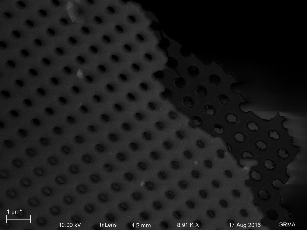
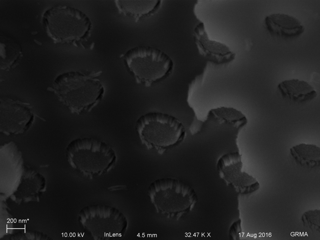
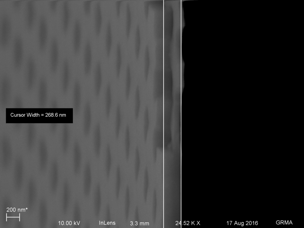
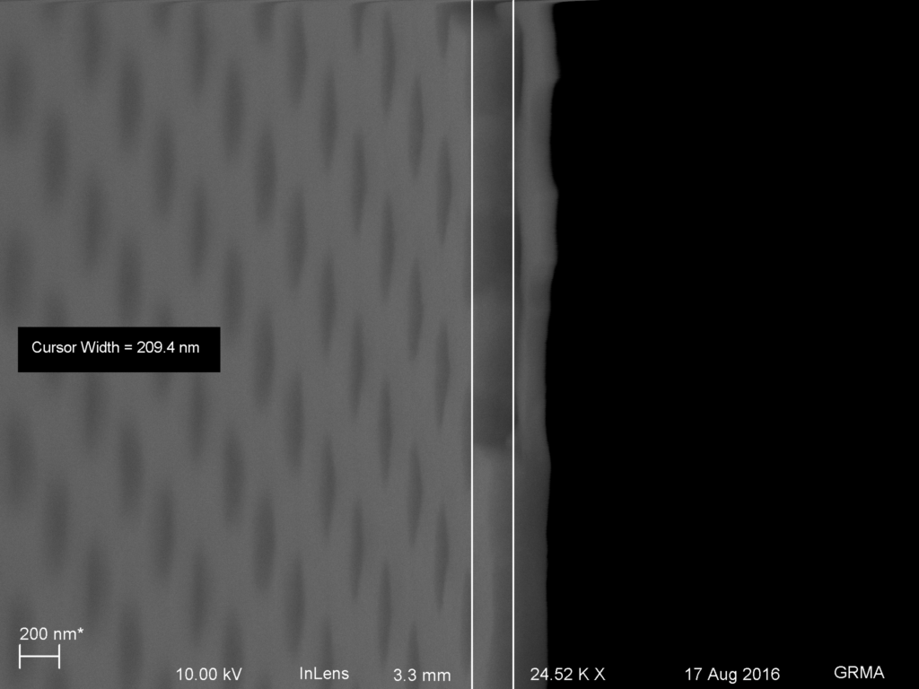
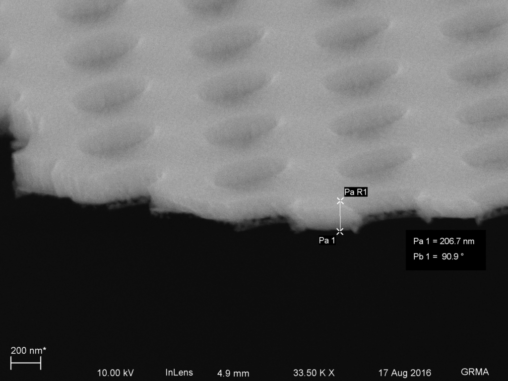
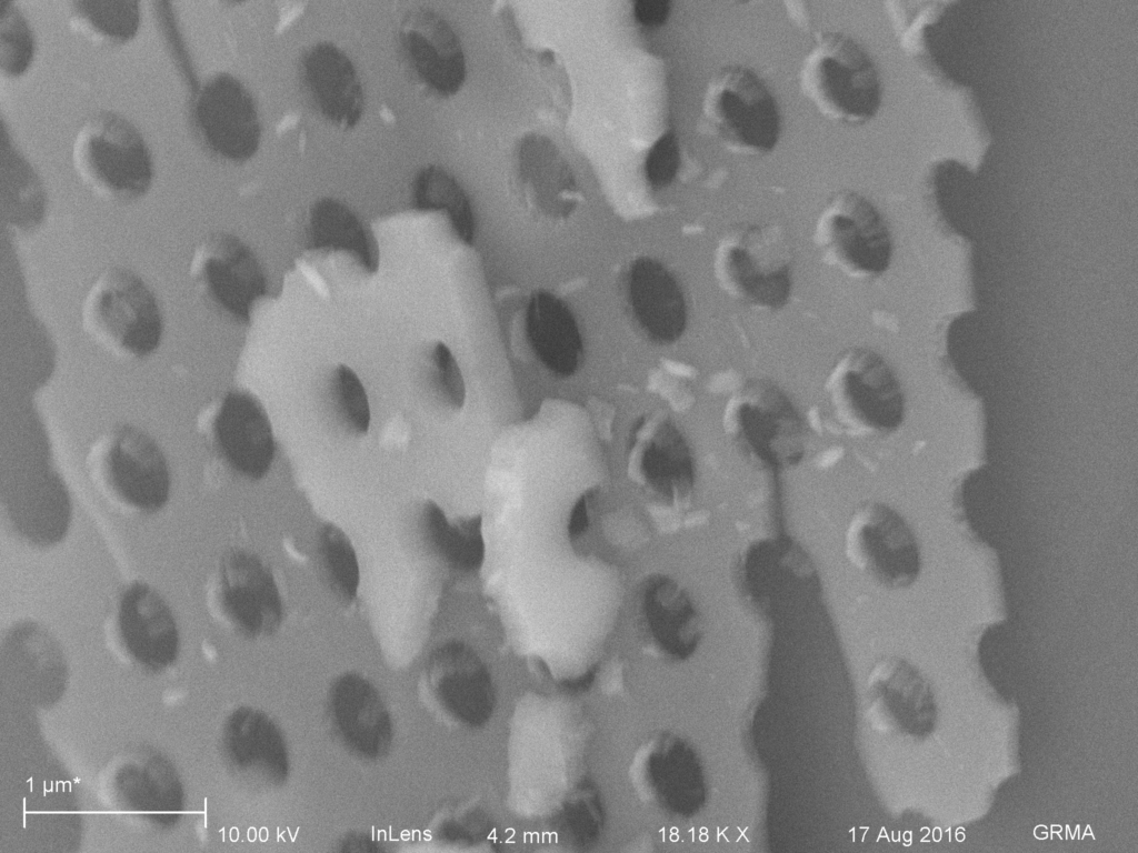
In terms of yield, I processed 25 chips. 24 made it through evaporation completely intact, and since these chips had 5 slots (3mmx0.1mm), 123/125 Windows in total. Etching wise, I have only processed 3 chips (15 windows) and while none were totally intact, 10 windows were remaining (10/15). We will see if the etching holds up. It seems to be one of the 3 middle windows that fail, not the edges, which may indicate an etch pressure effect.