Electrical Characteristics of Silver/Alumina NFTs
Just before BMES I was finally able to electrically characterize my NFT chips. Previously, I had been trying to collected IV sweeps using the following circuit:
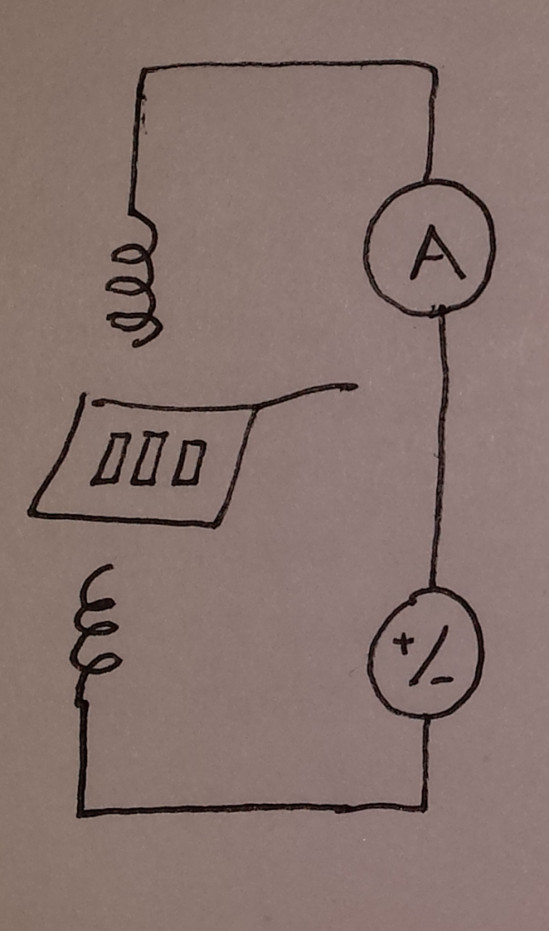
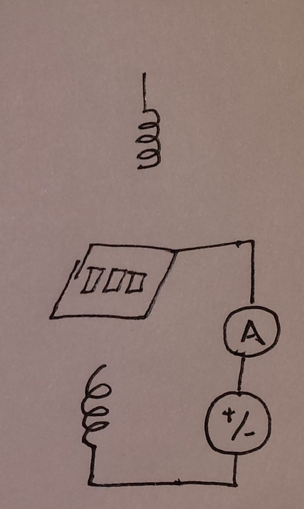
The problem with this was that, as Jess discovered, the membranes have almost no electrical resistance in this configuration, and I was essentially shorting out the circuit. This meant that my electrodes were ruined and my measurements made little sense. But after digging through the literature (and in particular this paper: Fabrication of nanopores with embedded annular electrodes and transverse carbon nanotube electrodes (pdf) which describes the cyclic voltammetry measurement in some detail) I realized the proper circuit was the following one:
In theory, taking an IV curve is straightforward. All you do is slowly increase the voltage applied to your chip while measuring the current and plot the voltage vs. current. Most labs do this characterization using a Keithley sourcemeter or the equivalent, which automates the process, and though we recently received one of these in the mail, we did not yet have it when I made these measurements. Without a sourcemeter, I instead took a series of videos using my smartphone where I turned the voltage knob on our power supply to change the voltage applied to the chip at 0.1 V/s. Further hampering this effort was the fact that the DC power supply we have only supplies positive voltage, and so midway through the experiment the leads would need to be flipped. My sequence of actions for a measurement was as follows:
1) begin recording a video on my smartphone with the readouts to both the Agilent voltmeter (set to measure amperage) and the DC power supply clearly visible.
2) turn on the DC source. After letting the source stabilize at ~ 0 V for 5 seconds, turn the knob at a rate of one ‘click’ per second, with the machine set to increase/decrease the applied voltage by 0.1 V/click.
3) reach 2 V. Begin lowering the applied voltage.
4) reach 0 V. Flip the leads so that the sign of the voltage applied is flipped. Turn the knob at one click/second
5) reach -2 V. Begin lowering the applied voltage.
6) reach 0 V. Turn off the machine.
7) upload the video to my computer and carefully record the voltage vs. current into excel.
A representative video of steps 1-6 is below:
This worked, but it was a miserable process, with a single recording taking >10 minutes to input into excel. Now that the sourcemeter is here hopefully I will never have to do this again. That said, the results I got were exciting.
First, here’s the IV sweep I got for a platinum chip.
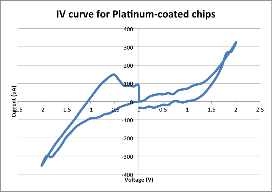
There’s a lot of weirdness here that I won’t try to explain (why the hump at -.5 V?) but the important thing to note is the current at +/- 2 V. It is +/- 300 uA, respectively.
Here’s a chip with just 12 nm of silver (no alumina):

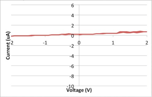
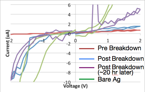
Now, if we make the same measurement using silver and alumina chips we get the following:
Or, the same image zoomed out:
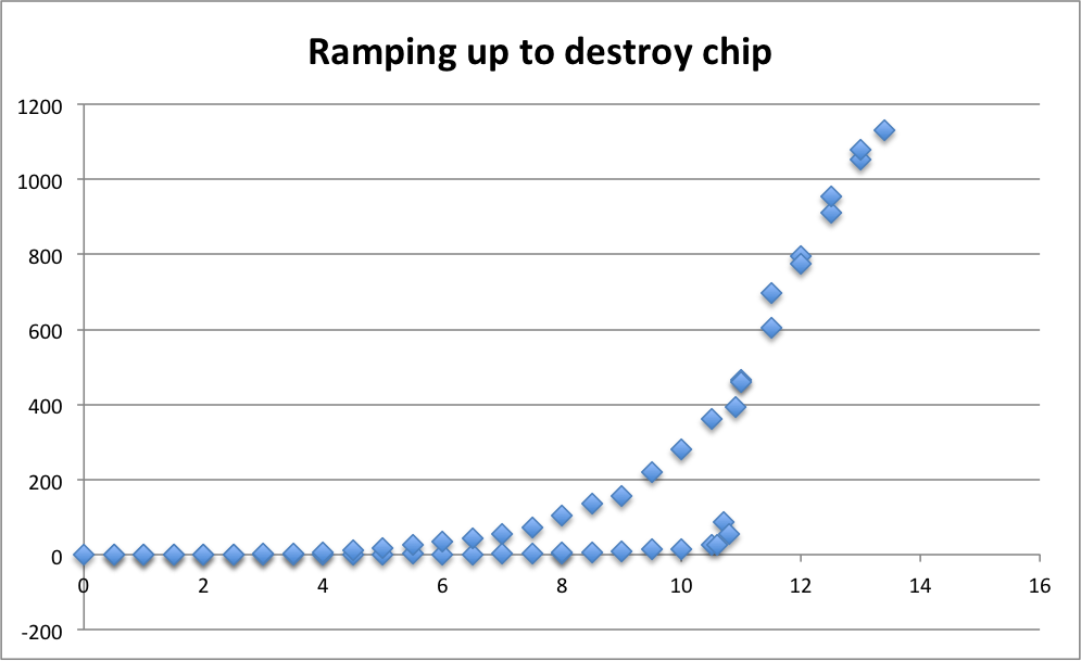
Next, I popped the chip by putting 10 V into it. This causes the dielectric alumina layer to break down.
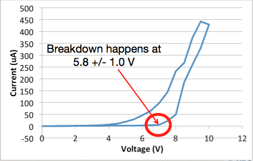
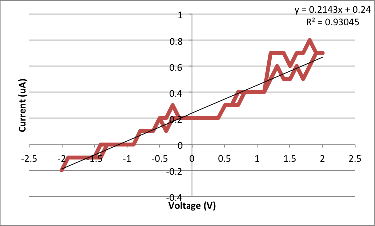
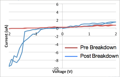
Making another IV sweep reveals that the chip has in fact been popped.
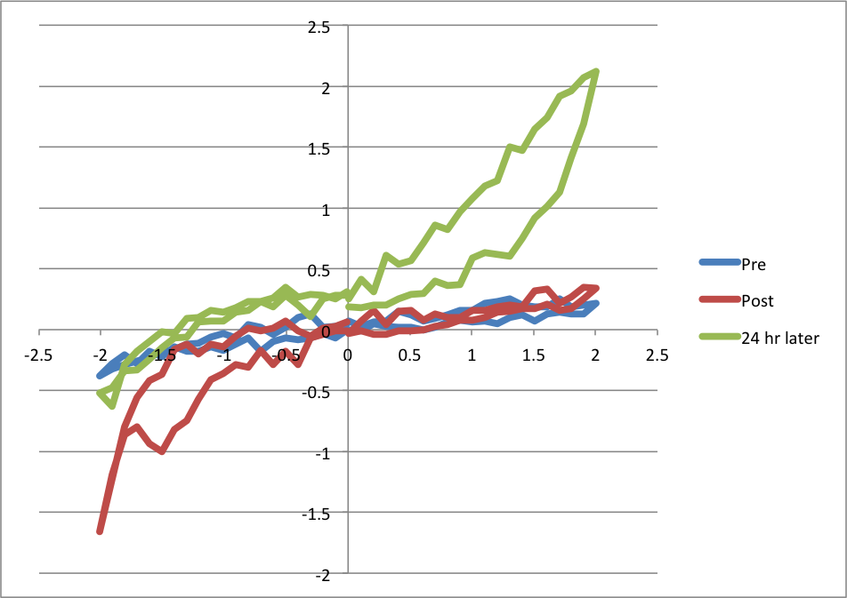
I repeated the experiment twice more to get some statistical power:
Chip 2:
Chip 3:
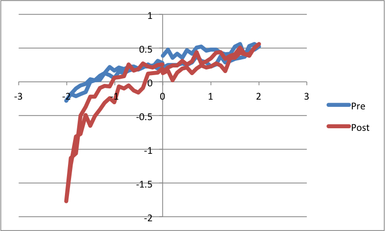
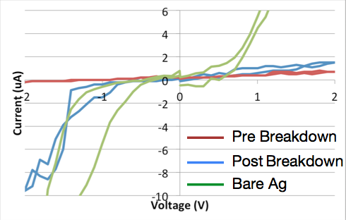
I believe this demonstrates that the chips are indeed insulated from the bulk before they are popped. This paper (Investigation of Al2O3 Deposited by ALD as Passivation Layers for InP-based Nano Lasers – pdf) found that 10 nm of alumina had a breakdown voltage of 5-7 V, which is in agreement with this data. It’s interesting that freshly popped chips only seem to leak current when a negative voltage is applied. My hunch is that this is due to electrochemistry – perhaps because the solution hasn’t had time to form Ag/AgCl on the surface of the silver film, charge can enter the film but can’t leave it.
Before I ran this experiment with NFTs with leads attached, I was having trouble attaching the leads. I ran the experiment without using silver epoxy and just pressed a silver lead to the chip surface. Cross-chip resistance measurements were ~35 M 
Pre:

“popping”:
Post:

Finally, here is the raw excel spreadsheet data (IV sweeps). I won’t upload the videos but I have them on my hard drive.