TEM images of NPN show a variety of nanostructures
As the title states, I have been making TEM images and reconstructions from a variety of NPN materials. I hope to correlate the underlying nanostructure with SERS activity eventually. These images show many different porosities, topographies and pore shapes. Wafer 1236 has been the bulk majority of my npMgF2 fabrication for my SERS experiments.
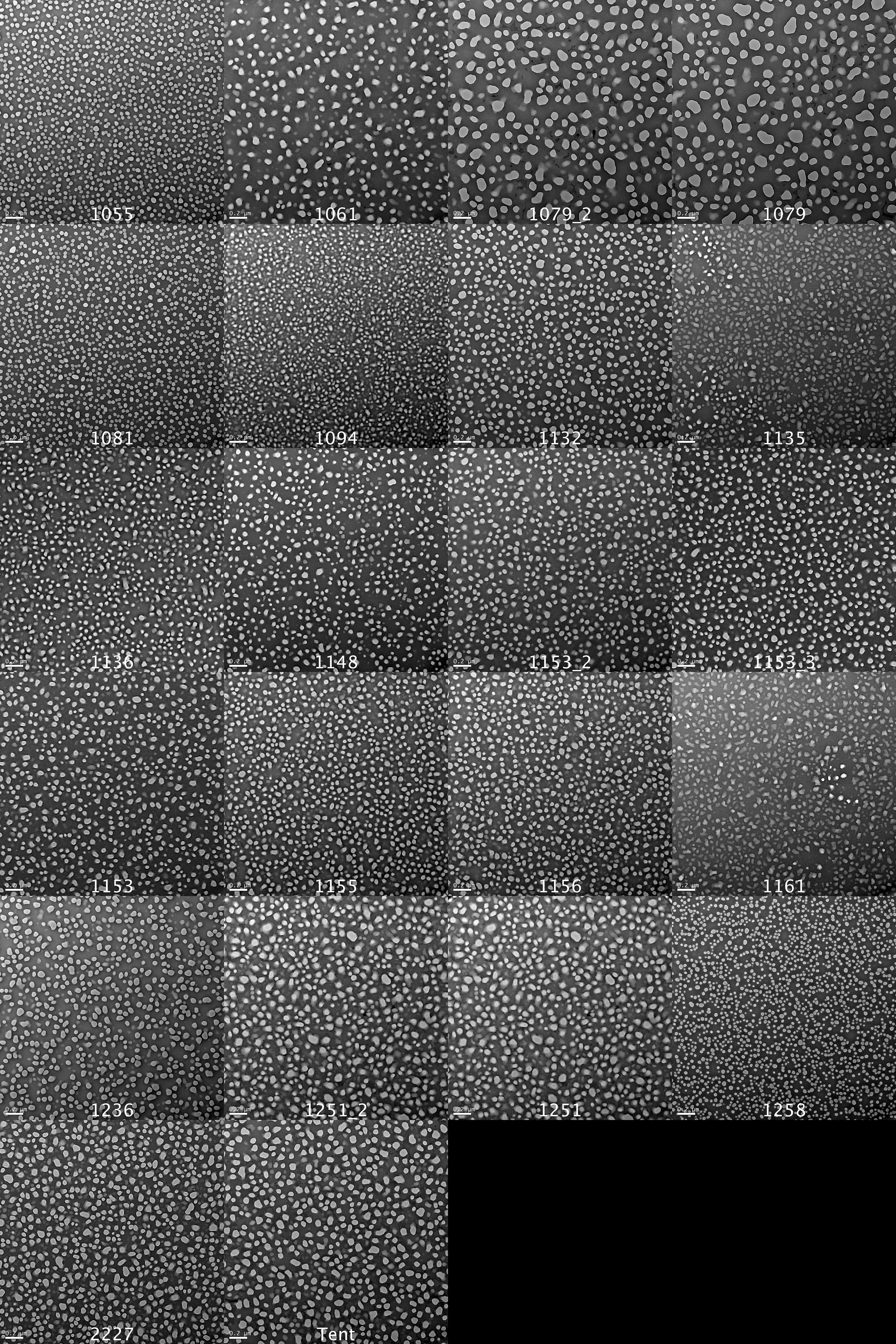
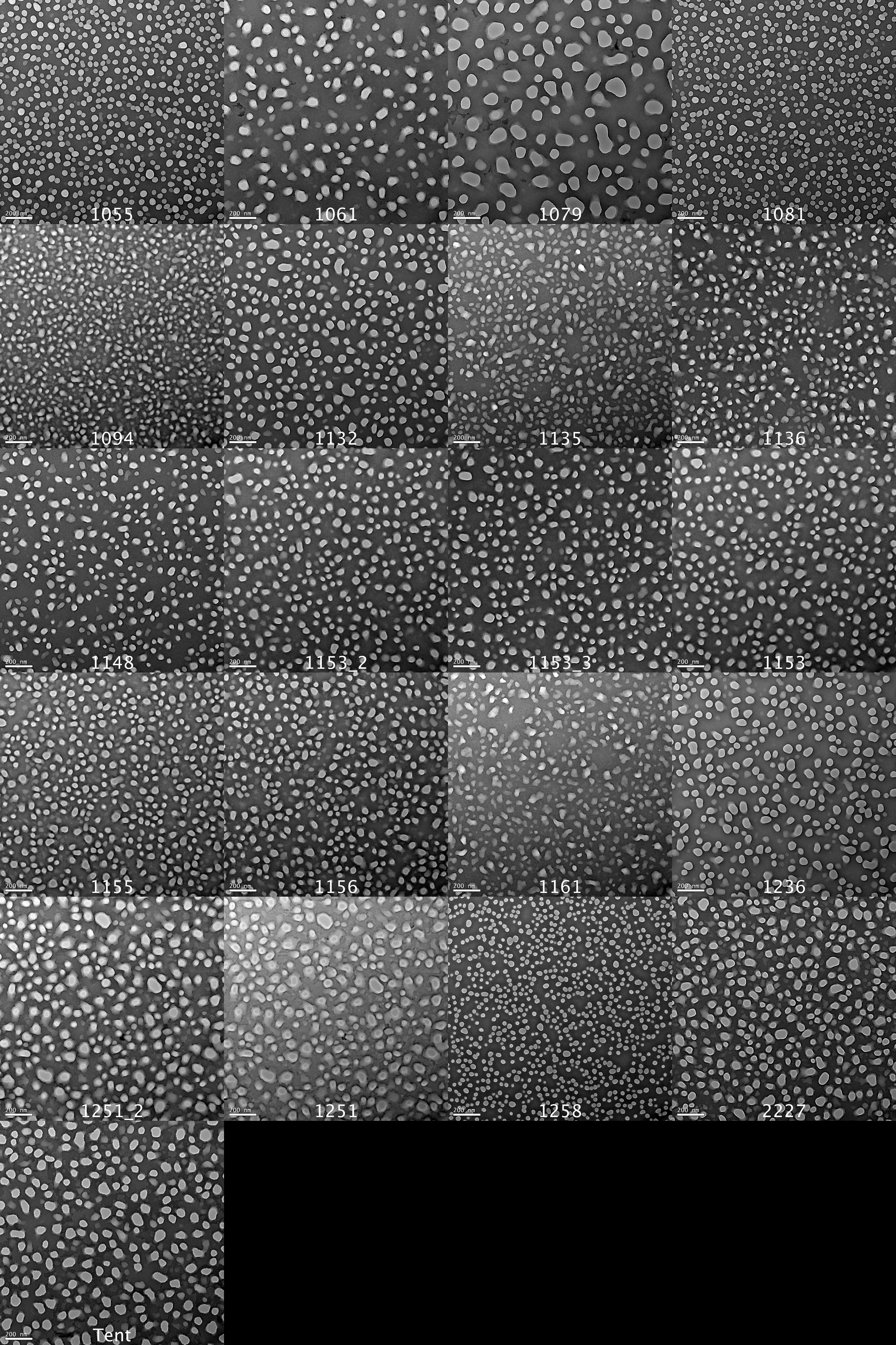
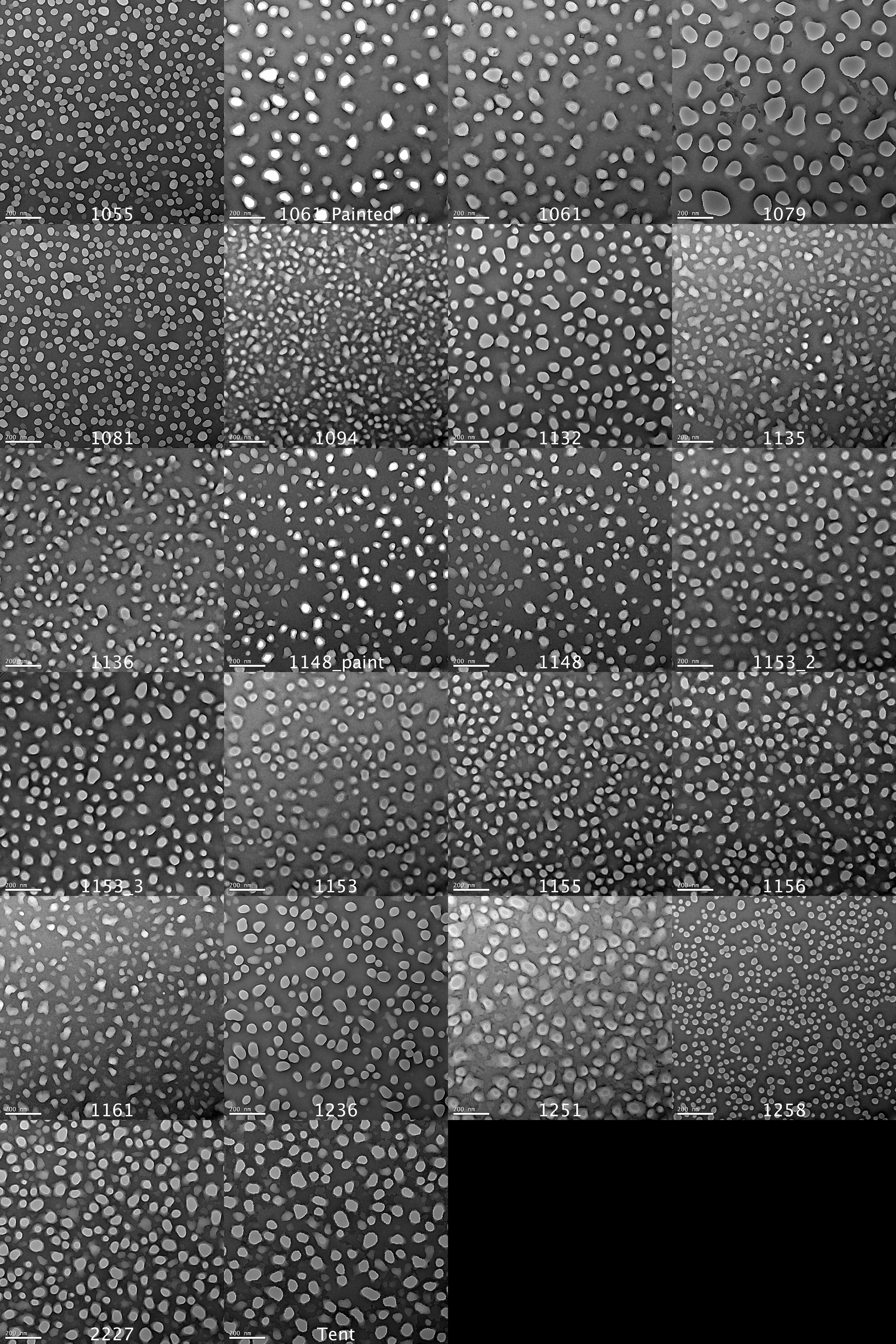
I have also been creating tilt stacks for my eventual tomogram reconstruction. I align the images using SIFT correspondances in Fiji, and then reduce the size, copy the stack, reverse the duplicate, and concatenate the stacks to create the looped gifs you see below. They also show a wide variety of structure at 64kx.
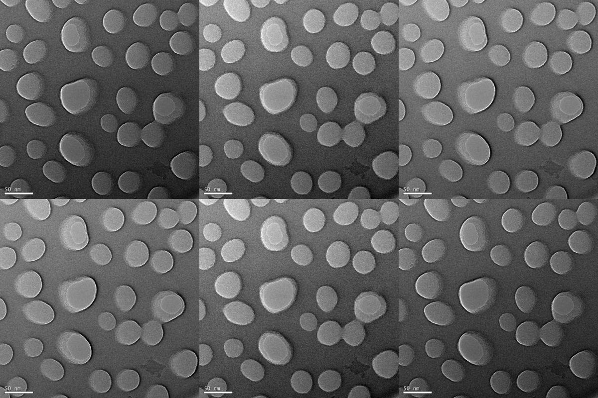
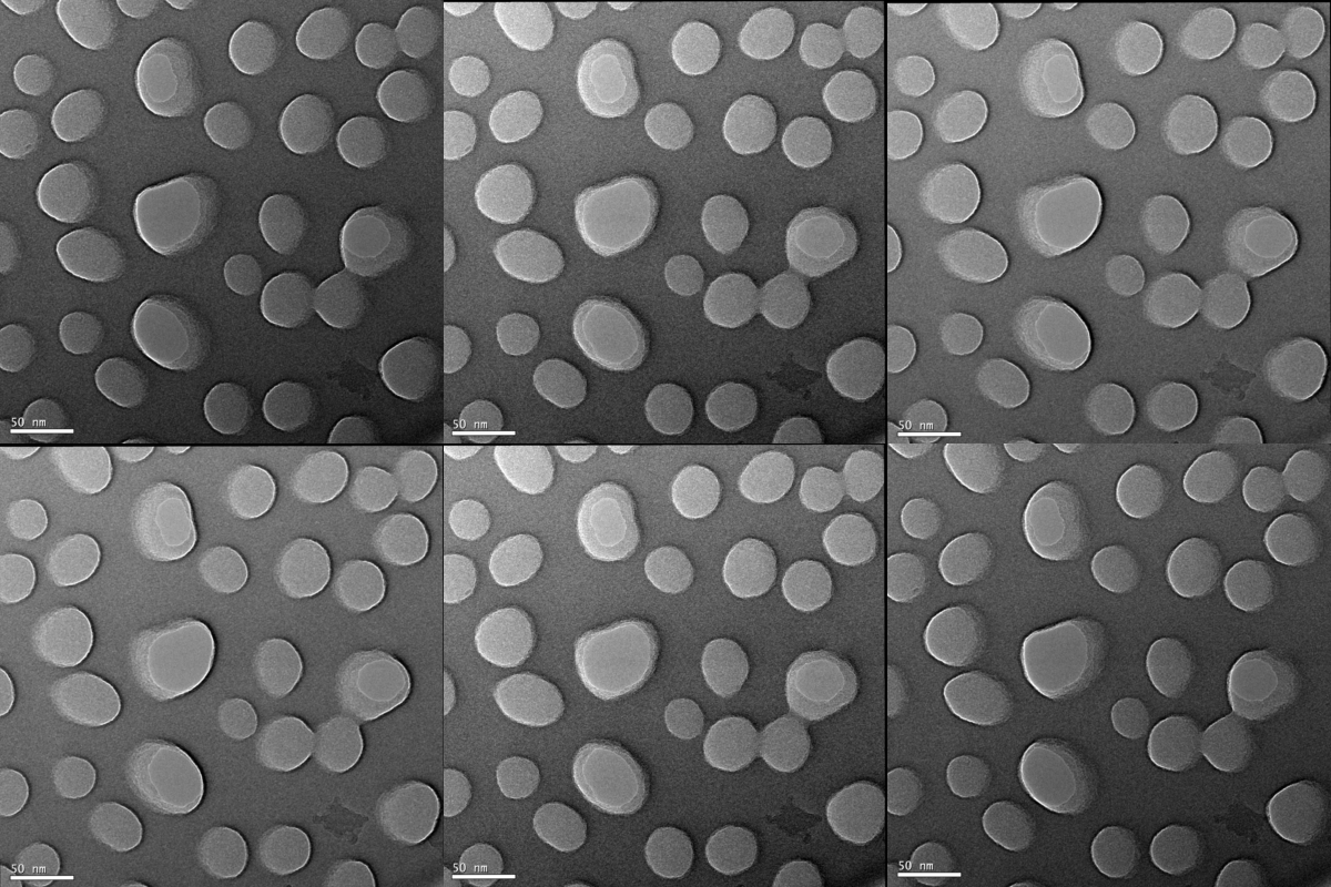
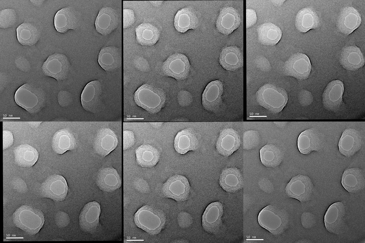
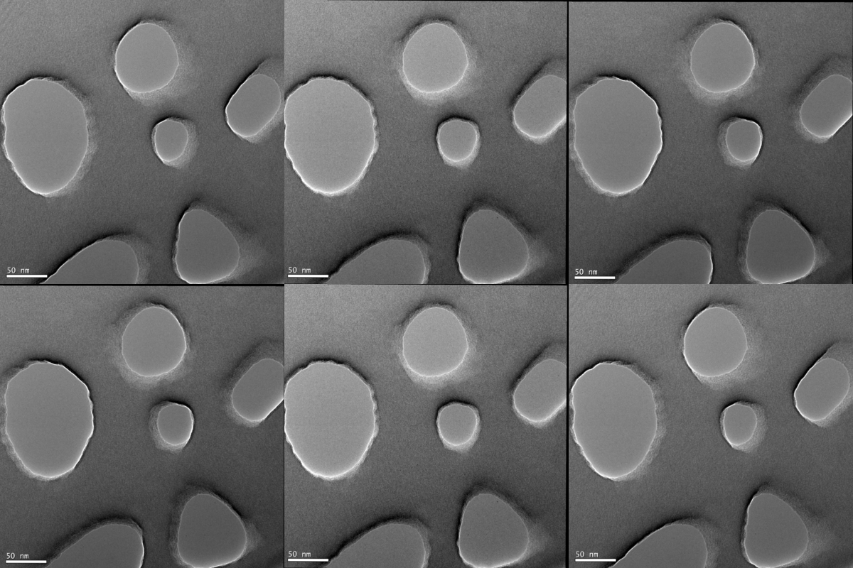
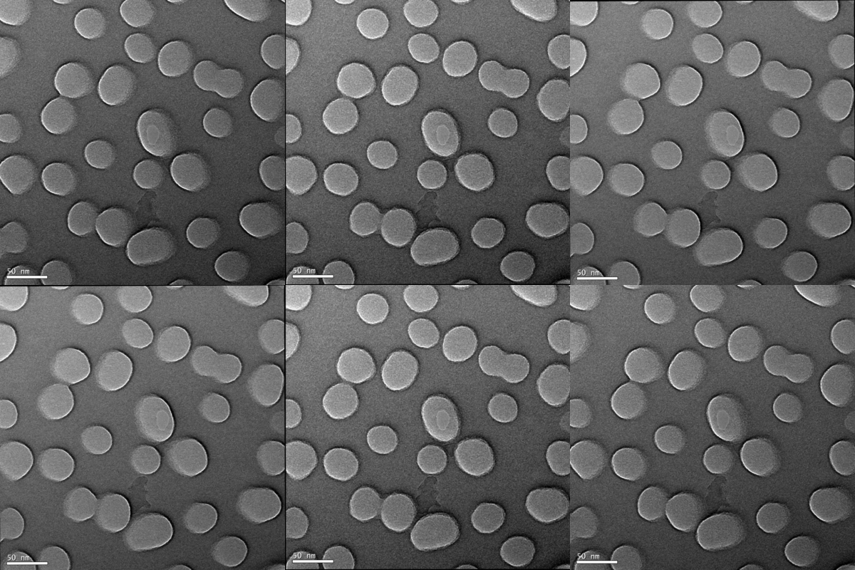
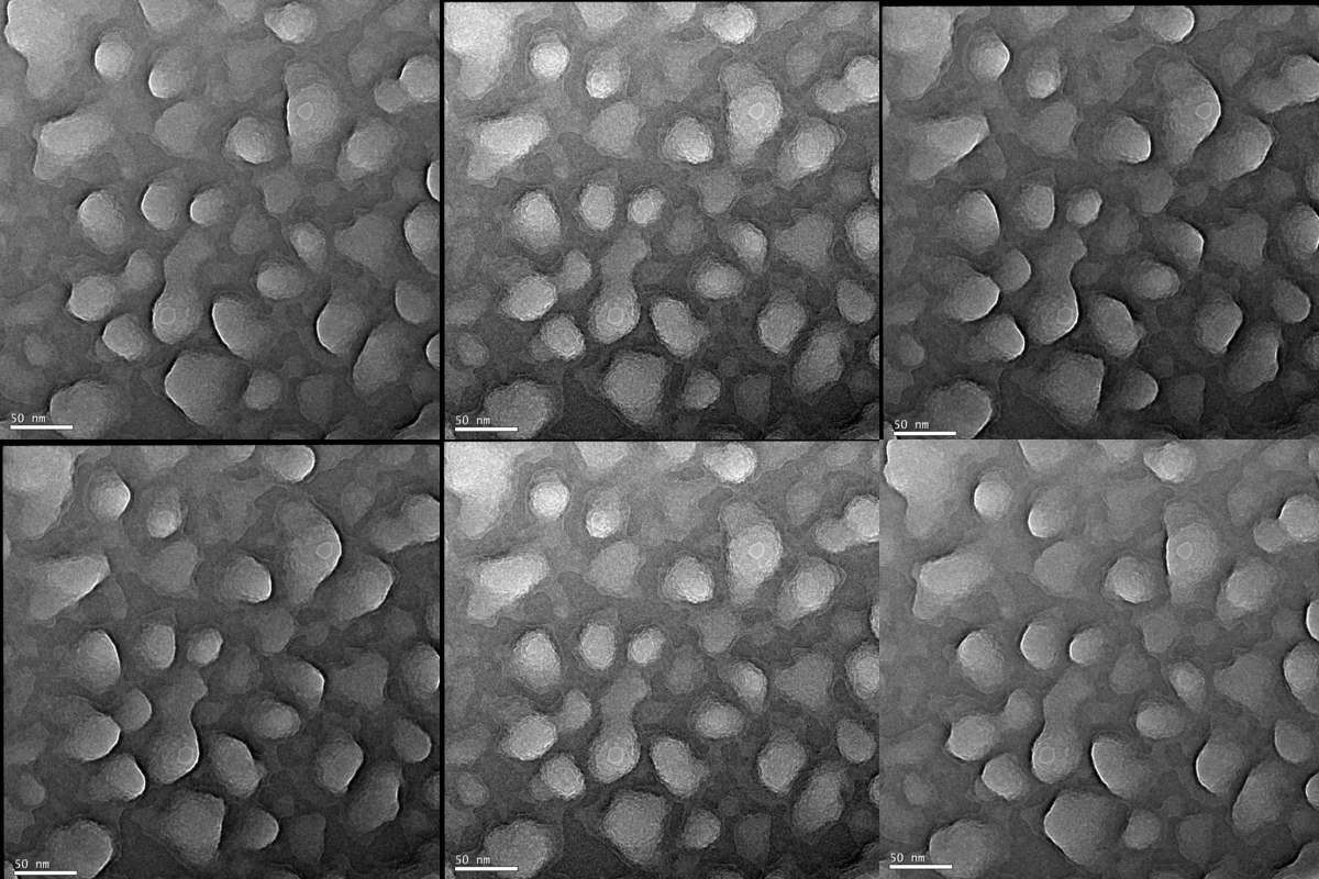
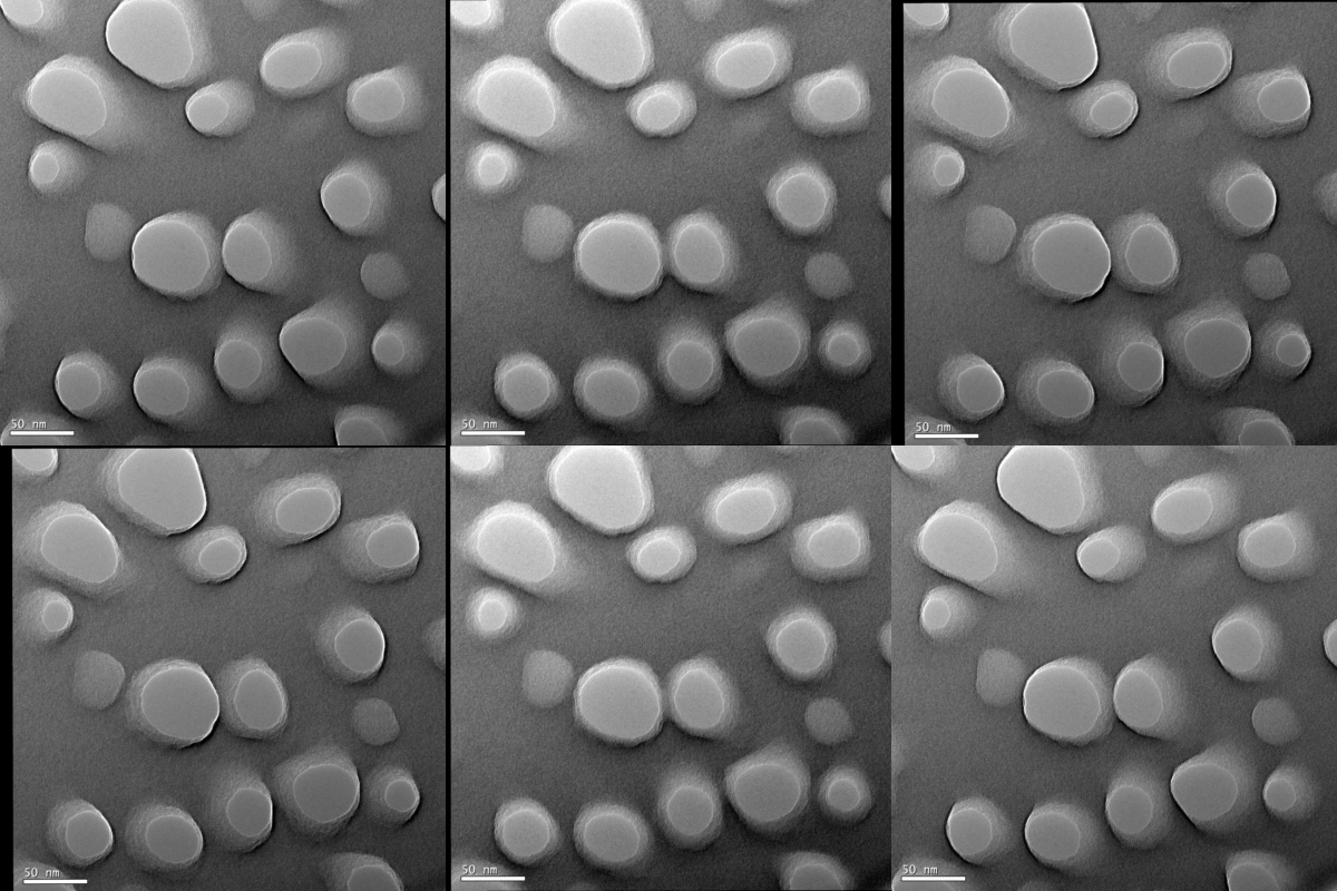
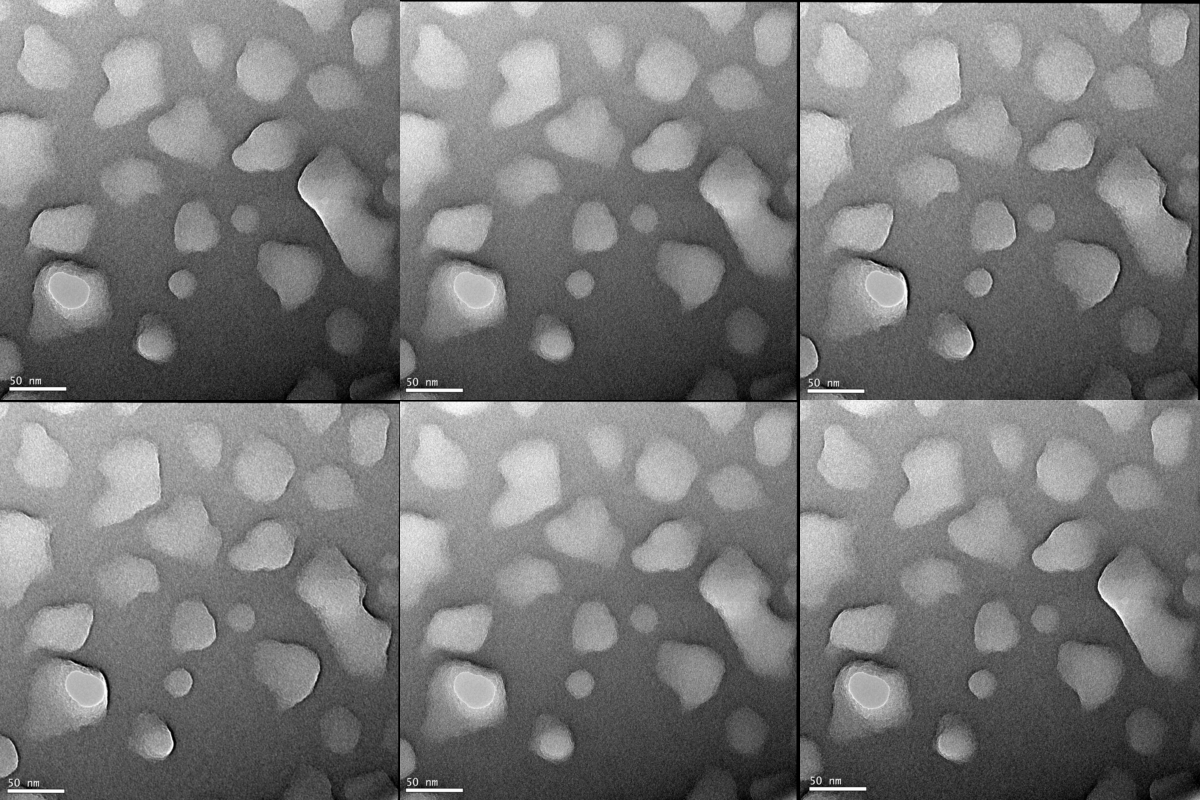
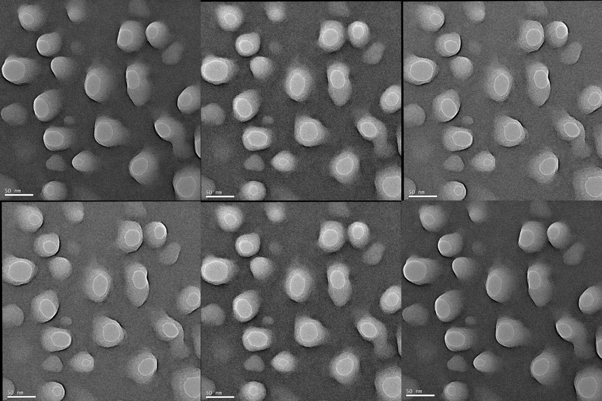
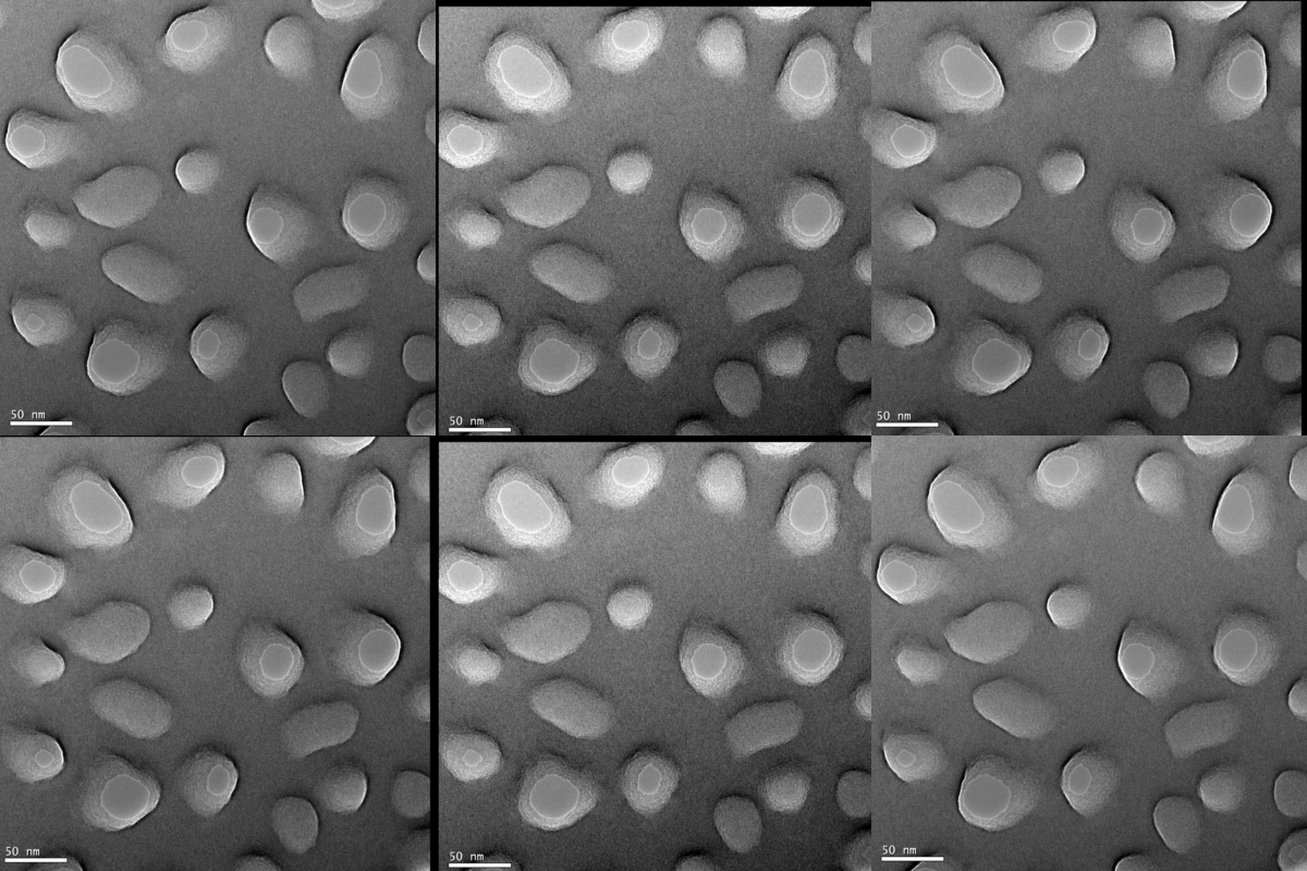
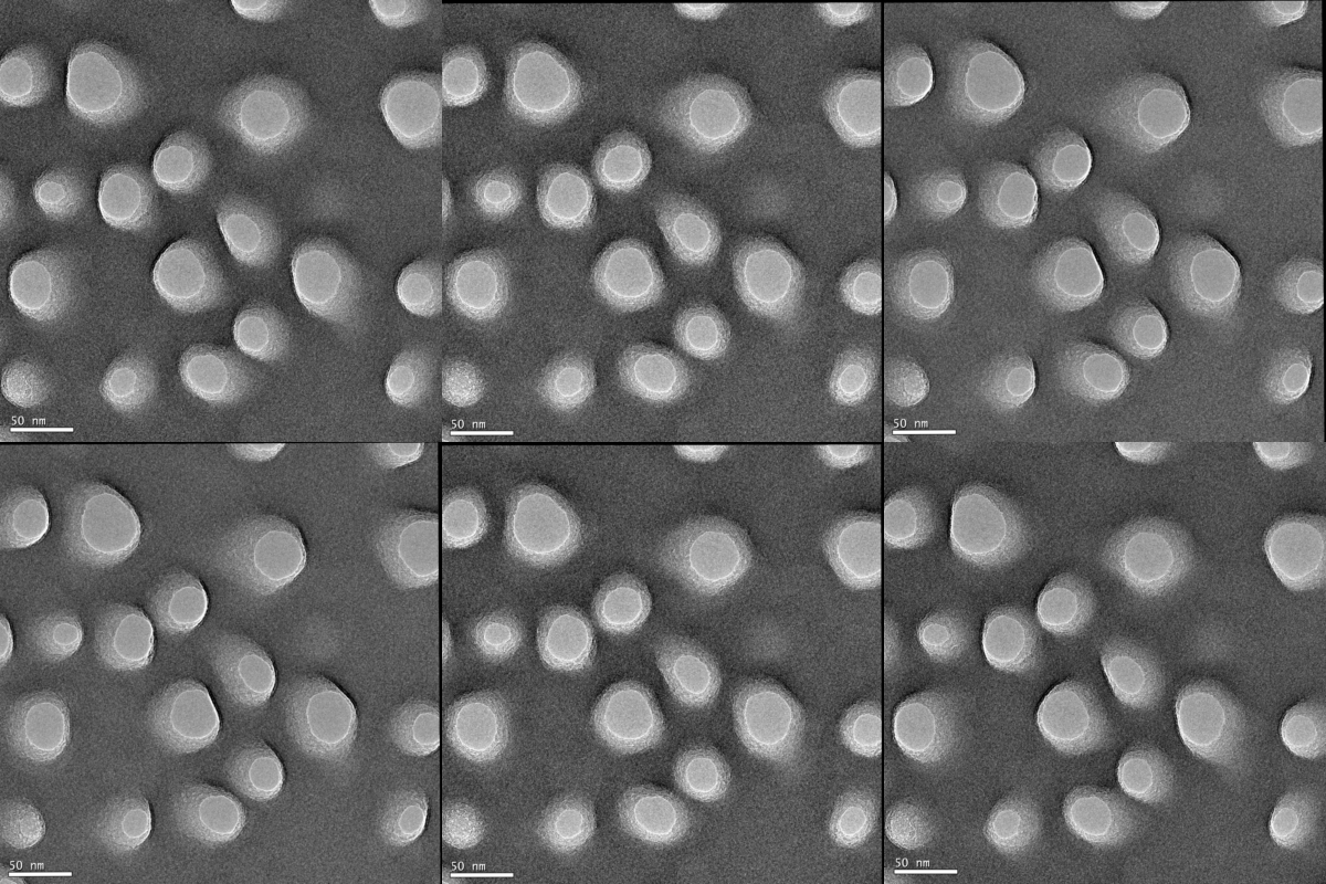
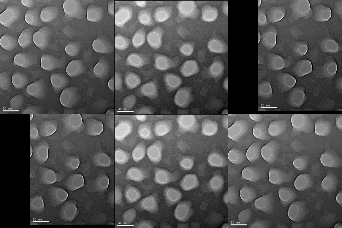
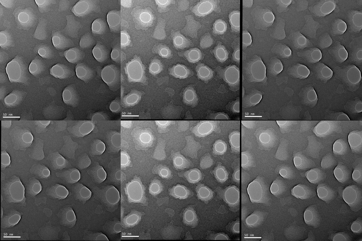
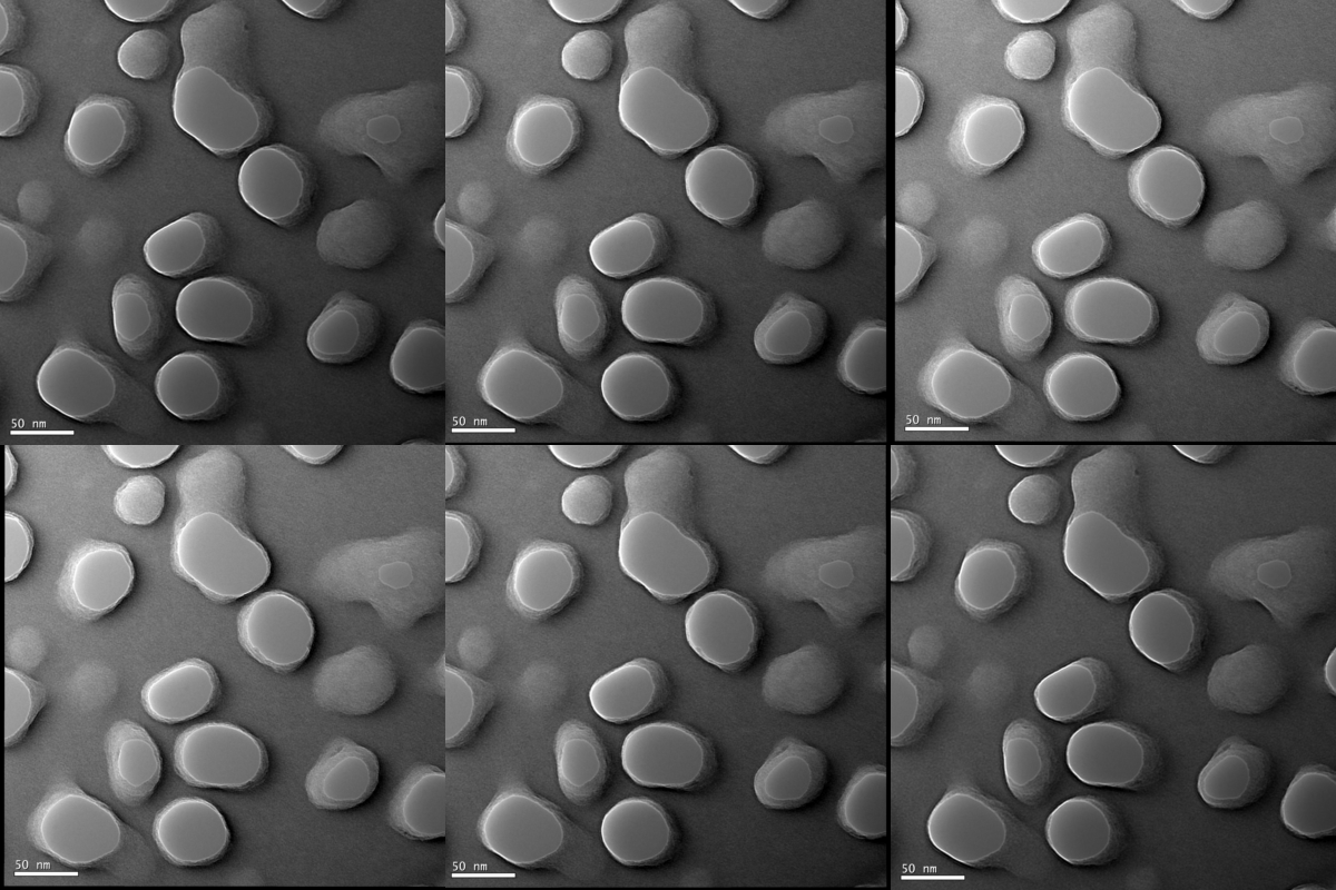
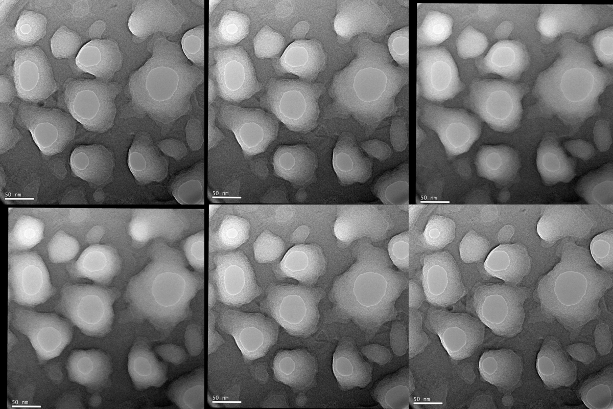
In the tilt-shifted images it’s clear that many of the structures aren’t through-holes. Is that just a timing issue with etching, or something more fundamental?
It’s more a timing issue with etching, but there are some fundamental properties of the NPN fabrication that cause some of the pits. Basically, the NPN is formed from another structure that may have partially etched holes in it; these are transferred to the NPN layer with varying amounts of fidelity. By over etching, we can turn some of those original masked pits into through-holes, at the expense of merging some pores. I have shown previously with my blog posts that we can partially etch the NPN to open up some of the lost porosity, by thinning out the membrane.