Monolith X-sections
As the title states, these are images from the monolithically fabricated devices used by Kyle and Vincent in Ottawa. These devices were fractured with tweezers, then tilted and metallized with 5 nm of Pt, mounted on carbon tape.
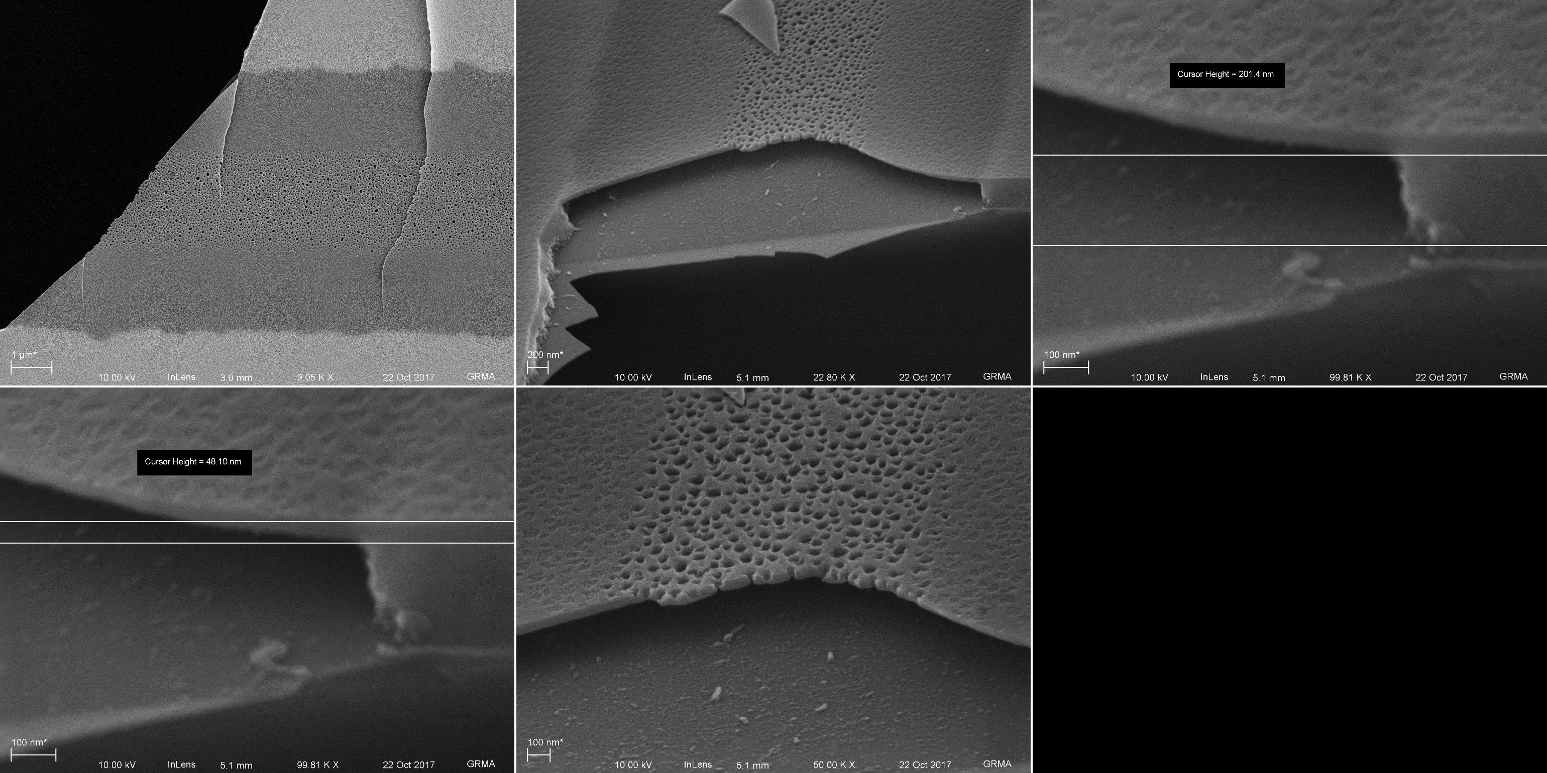

As the title states, these are images from the monolithically fabricated devices used by Kyle and Vincent in Ottawa. These devices were fractured with tweezers, then tilted and metallized with 5 nm of Pt, mounted on carbon tape.
We have long maintained that we can capture more analyte from a sample using a flow-through configuration compared to a tangential configuration. We can confirm this view quantitatively by measuring the amount of material captured on the membrane with equal source flow rates. Additionally, one of the advantages of a silicon-based platform is that we can…
I’ve added a page on cell culture applications to the knowledge wiki. Watch this page and edit it if the topic is of interest to you. Remember the wikis provide a place to comment on the changes you make … and to compare and restore prior content … … so don’t be shy.
I recently presented an update at the HCIC User meeting on 11/10/23 detailing our efforts in exploring the use of optical tweezers to perform microrheology in type I/type III collagen hydrogels. These hydrogels are of interest for in vitro models such as the hToC and we would like to explore the viscoelastic changes caused by…
PLEASE read this journal article for NRG on Tuesday March 18th @ RIT (PDF links are at the bottom) Surface Chemical Modification of Poly(dimethylsiloxane) for the Enhanced Adhesion and Proliferation of Mesenchymal Stem Cells Shreyas Kuddannaya,†,§ Yon Jin Chuah,‡,§ Min Hui Adeline Lee,‡ Nishanth V. Menon,‡ Yuejun Kang,*,‡and Yilei Zhang*,† I’d like to discuss this paper…
Update: After doing several measurements again, it appears that the data shown below were not repeatable. It is believed that these data were just the artifact. Please see my new blog post “Flow Sensing and Energy Harvesting Capabilities of NPN Membrane” for a new data set. Here are the streaming potential measurement data for NPN membrane…
Yuchen and I have been tasked with integrating TEER electrodes into the Cytovu format. The general idea was to fabricate the TEER electrodes similarly to what I have done already, then add them to the current Cytovu device, using UV ozone bonding and PDMS (to cement in the top electrode). I drew some electrodes to…
Comments are closed.
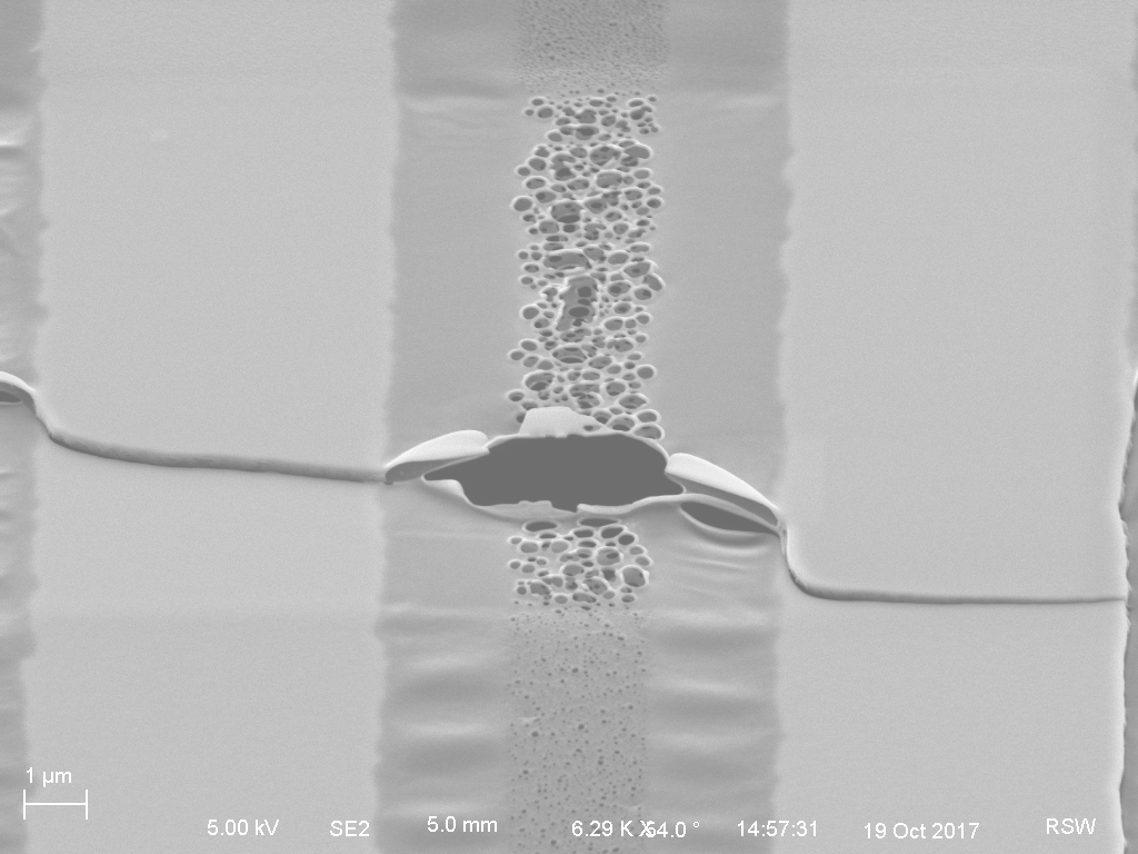
Thanks for getting these Greg. A few comments: The first montage, you point out the large under etch…this was a known condition that was expected. Its due to the XeF2 gas, which is very isotropic. As for the debris, this is also a known condition, also due to the XeF2, I believe this is due to contaminates in the poly-Si as deposited (at RIT) and because the selectivity of XeF2 is absurdly high, it does not etch at all. I do not think these ‘crumbs’ would interfere with pore formation since they are not continuous, and since the pores are actually enlarging, they probably are being dissolved in the KCl solution (and therefore not plugging the pore).