UV-vis Spectrophotometer Measurements on NPN
We’d like to get verification of the absorption spectra of our npAu/npMgF2 SERS structure. The SERS effect should occur where the absorbance is maximized.
Total Light = Absorbance + Reflection||Scattering + Transmittance
Last Friday, I had the opportunity to work with Jennifer Kruschwitz who possesses a Konica-Minolta integrating sphere spectrophotometer from 380-740 nm (10 nm increments). It’s primarily made for examining the reflectance and transmittance of paint swatches/filter glass, but it has a 3x5mm aperture which is reasonably sized for our chips. One concern with my SERS chips is that they have only a small active area (9x 0.5×0.5 um windows = 0.0225 mm^2). I have been using chips for these experiments on the order of 1.5 mm^2 to get decent signal.
I metallized chips using the Denton Sputterer (15mA current, 100 mTorr, 0.1 nm/sec) for varying amounts of time to produce Au layers of different thicknesses. The chips became more opaque as I added more Au, by eye.
I made a few preliminary measurements of reflectance on partially etched NPN, after cribbing together a reflectance mount for the system, using carbon tape and a black aluminum plate.

This week, I’ve made a few measurements on the transmittance side of things. 1148X NPN (labeled as 1148 in a 4″ cassette, need to verify with TEM) is some 5 slot NPN, with total area = 1.5 mm^2. I created an aperture for the chip to sit on with an index card and carbon tape.
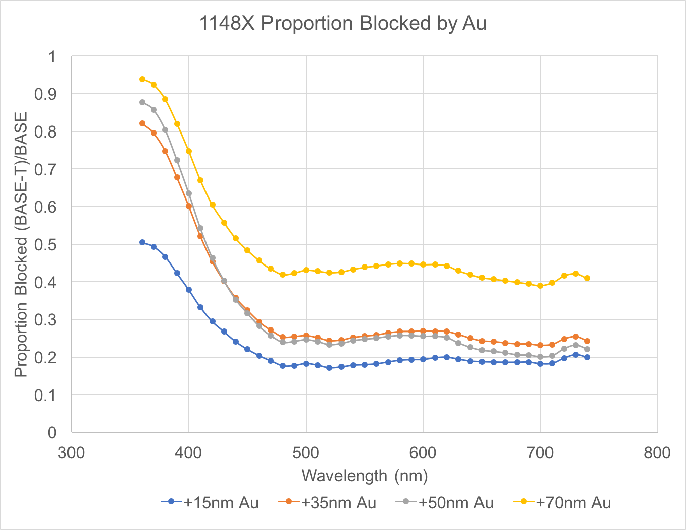
I can probably decrease the error of my measurements by improving aperture mount (if light leaks in underneath it impacts the transmittance). More work to come.