Design and fabrication of the microfluidic flow module
Introduction
Sepsis is a serious condition where unregulated systemic inflammation can cause organ failure and death. Recent evidence has also shown that sepsis can cause cognitive impairment in surviving patients. However, the mechanisms that cause sepsis-related damage to the brain are challenging to study with the current in vitro tools. In this project, our goal is to develop a blood-brain barrier model with defined compartments that comprise the blood and brain sides of the neurovascular unit to study circulating factors and inflammatory status in the system.
In this post, we describe our progress developing a “plug and play” microfluidic flow module and integrating it with a platform known as µSiM (Fig. 1) to recapitulate critical features and functions of the human BBB. The µSiM offers barrier tissue formation capabilities with high-quality imaging, tunable porosity, and controlled thickness to ensure cell-cell communication across the interface. The microfluidic integration will enable the static µSiM to be converted to a flow module that will impose physiological shear stresses to endothelial cells and allow controlled introduction of secondary cell populations (i.e., monocytes and neutrophils) to the system.
The initial design of the platform and its fabrication method is described (Fig. 2,3). A major goal is to provide a simple method to convert the static uSiM to a flow enabled system that can be easily used in our collaborators’ labs.
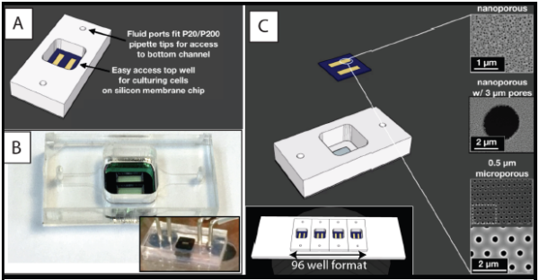
Fig. 1. A) schematic representation of the µSiM platform, B) Assembled µSiM with flow cell capabilities, C) Images show available nanoporous membranes that can be integrated into the system.
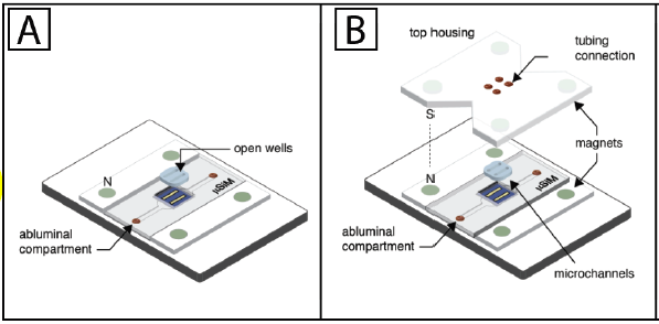
Fig. 2. Schematic representation of integration with A) introduction of a molded microfluidic device, B) magnetic sealing.
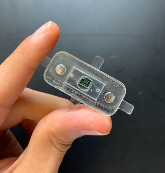
Fig. 3. Schematic of the magnetically assembled prototype
Methods
The microfluidic chip was fabricated using the standard soft lithography technique. The photoresist (SU-8 3050, Kayaku Advanced Materials, Massachusetts, USA) was spin-coated to a thickness of 200 µm on a 4” silicon wafer (University Wafers, South Boston, USA) and was followingly soft baked at 95˚C for 45 minutes. Then, the photoresist was exposed to UV (250mJ/cm2) through a high-resolution printed photomask. Next, post-baking was carried out for 1 minute at 65˚C and 5 minutes at 95˚C. Finally, the wafer was submerged in SU8 developer for 30 minutes under manual shaking. The wafer was cleaned with IPA and dried under an air stream before storage.
In order to obtain chips with a clover shape, a poly(methyl methacrylate) (PMMA) divider was laser cut and attached to the silicon mold with a pressure-sensitive adhesive (MP467, 3M, Saint Paul, USA) (Fig. 4). A 10:1 prepolymer base to crosslinker ratio mixture was mixed then degassed in a vacuum chamber for 45 minutes (Sylgard 184, Dow Corning, Midland USA). The degassed prepolymer solution was then poured over the SU-8 mold and cured for 1 hour at 70˚C on a hotplate. PDMS channels were extracted from the model, and their ports were punched using a 1mm biopsy punch.
Upper and bottom housings are fabricated by laser cutting PMMA. Two parts of the upper housing are attached together using a pressure-sensitive adhesive (MP468, 3M, Saint Paul, USA). Then, Nickel plated magnets (K&J Magnetics, Pennsylvania, USA) were inserted in the housings.
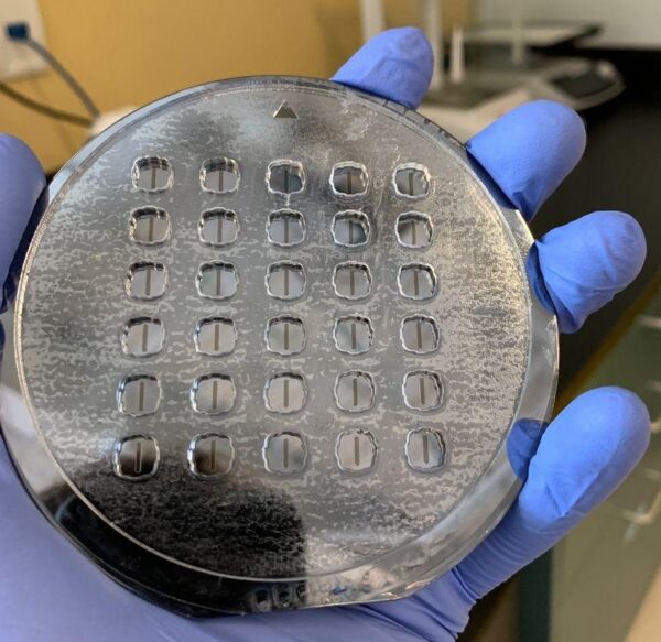
Fig. 4. Schematic of the silicon mold
Results
As it is shown in Fig. 5, the platform comprises four components, including bottom housing (A), µSiM (B), microfluidic chip (C), and upper housing (D). The magnetic contact between the bottom and upper housings provides the latching mechanism and sealing of the microfluidic chip. This platform is reversibly sealed, and it can be easily assembled and disassembled (Video 1).
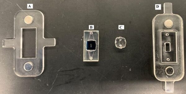
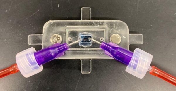
Fig. 5. Components of the platform
The contact area of the microfluidic chip and membrane chip is shown in Fig. 6. The width of the channel was increased to 1.5 mm to prevent the breakage of the membrane because of contact between channel edges and membrane. Initial leakage tests were successfully conducted, and the platform showed no leakage. In the future, the flow and shear distribution over the membrane will be simulated by Comsol and validated experimentally using the particle image velocimetry (PIV) method. Also, leakage tests will be conducted over multiple samples to approve that devices are leak-free.
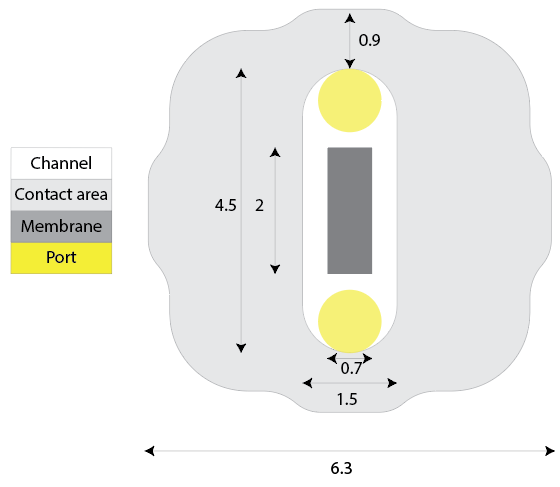
Fig. 6. The interface of the microfluidic chip and membrane chip