Top SiO2 Thickness Experiment (2)
Last week, I did another two wafers with different top oxide thicknesses to verify my hypothesis about the top oxide thickness effect on pores. The wafers were 20/15/03(bottom/middle/top) and 20/15/40. According to the hypothesis, the porosity of 20/15/03 would continue decreasing, where for the 20/15/40 structure, the porosity might drop. Same tip I used before, I redeposited 17nm oxide on the thinner wafer to protect Si layer before etching. Other processes including deposition parameters were same as the first top oxide experiment. The following is the TEM micrograph.
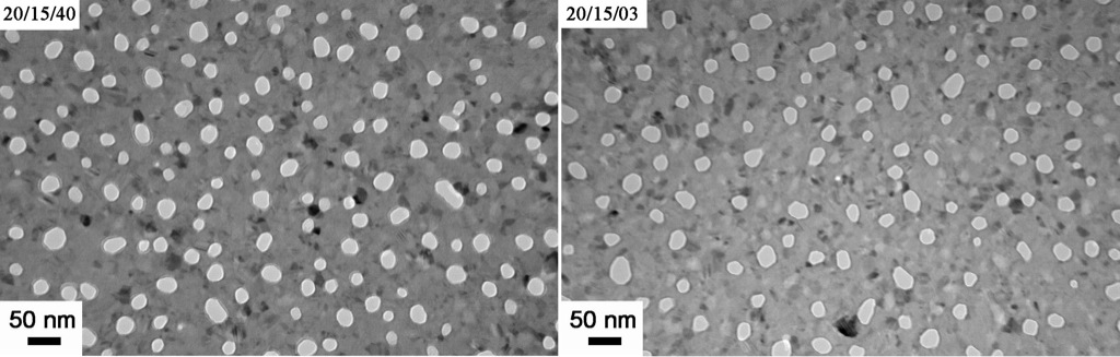
The porosity and pore diameter is 13.1% and 21.5nm for 20/15/40 structure where 10.4% and 21.3nm for 20/15/03 structure. I combine these data with my previous experiment.
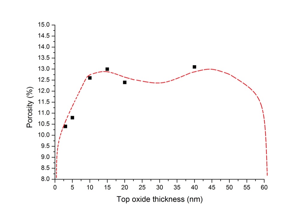
It can be seen that the 20/15/03 structure clearly fits the hypothesis. However, for the 20/15/40 structure, the porosity does not decrease but maintain at the second zone. Actually this is not surprising because it means that the 40nm thick top oxide is not thick enough to reach to the third zone that the porosity drops very fast with thickness.
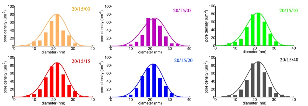
Next is the histogram of all six samples. It seems that the histograms of samples in second zone looks slight different from that of thinner oxide samples in first zone, which may indicate that the different thick top oxide would cause different stresses in the stack so that somehow affect the growth of crystals and pores. Further investigation in terms of strain and stress in three stack is needed.
The following graph is the pore diameter versus top oxide thickness. It can be seem that the average pore diameter does not change much with top oxide thickness.
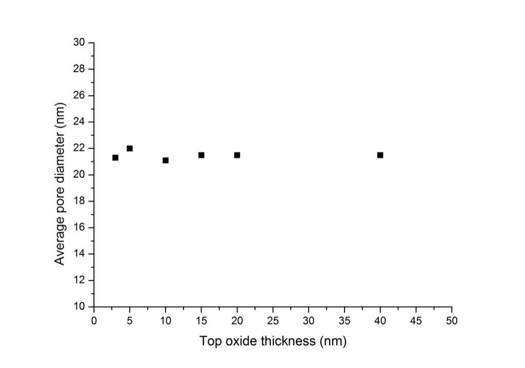
Up to now, I think it is safe to conclude the effect of top oxide. The top oxide is necessary to the pore formation. Without it, agglomeration would take place. Once the top oxide is there, pores would form during the annealing and the morphology would not change much with top oxide thickness. So top oxide is necessary but not the dominant factor to pore formation and pore morphology.
Next step, I would like to try a very thick top oxide structure to complete the third zone of the porosity vs top oxide thickness graph and then switch to bottom oxide series test.
very intriguing. You may be on to something really nice here. I m even thinking you might close to a publication….
Nice work, Joe.
What do you think is happening with regards to nucleation and growth as you vary the thickness in the oxide layer? Maybe there are some clues in the histogram? How does the roughness of the silicon film change, if at all, with the different thicknesses? Some AFM would be informative.
Hi Dave, thanks a lot for your suggestions and questions. So far, I don’t think the different thick top oxide would affect nucleation very much. Instead, the nucleation should be highly depend on the defect density, annealing temperature and so on. But when talking about growth, since different thick top oxide would cause different stresses in the stack, which would somehow affect the growth of crystals and pores. I checked the histogram of those samples and it looked to me that the histogram of samples in plateau (second zone) is different from that of low porosity samples. I’ll update this post with the histogram so we can have a discuss. Currently, I’m not very sure how does the top oxide thickness affect the stress state and I’ll dig into it as a follow-up.
As respect to roughness, I think you are right that the roughness may change and AFM would be a good choice to find it out. As my own guess, the thinner top oxide could not provide constrain as high as thick ones, so the roughness might increase with decreasing top oxide thickness. We’ll see in the follow-up.