Thin Film Electrode Creation
I have been trying to fabricate my own Indium Tin Oxide (ITO) electrodes on coverslips for the BBB device in order to minimize the working distance for any microscopy. Currently, I am using microscope slides that are way too thick (mm). Coverslips are generally about 0.2mm thick. I am using a combination of sputter, photolithography, and wet etching to make my design, though I may incorporate a RIE instead of a wet etch at a future date. The electrodes’ resistance must be minimized (I’m guessing sub 1 kohm each) to make good TEER measurements (minimizing the background resistance of the device).
Process:
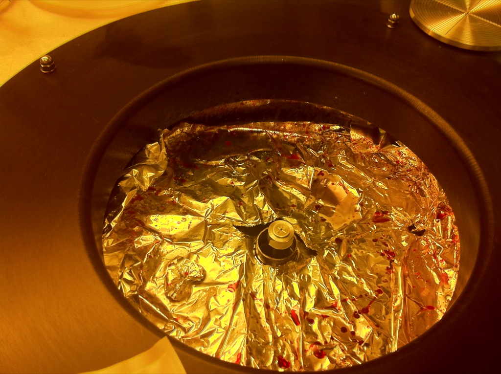
Sputter – Take bulk coverslips, clean using DI H20, sonication, Alcohol. Use a dehydration bake (150C for 10 minutes) to drive off water. Then use PVD Lesker ( to sputter thickness of ITO onto the slides (substrate gets up to 200C).
**In my initial run I used a 500 Angstrom recipe which gave me a “coverslip” resistance of ~800 ohms. I will probably have to deposit more material to minimize this resistance in the future. However, this will also decrease the transparency of the film stack. We will need to find a happy medium.
Mask Creation – I designed my 1mm wide, 1mm space, finger electrodes in illustrator, and used a few work arounds to get a dark mask pattern. I printed the mask on a 3M transparency sheet using the laser printer in the basement at 1200 DPI, transparency settings.
Note the line edge roughness and the speckle in the dark areas of the film. This is not a good mask, but should be sufficient for a first run. All the extra geometry and holes in the film will contribute to increasing the resistance of the etched electrode.
Photolithography – I used the spin coaters in URNano to apply photoresist to my slides, on the small single coverslip holder. First, HDMS application at 1500RPM for 30s, followed by a quick dehydration at 115C for 60s. Next, application of S-1813 positive tone resist at 1500RPM for 30s, followed by a soft bake at 115C for 60s. I applied about an eyedropper’s worth of volume to the center of the slide for both steps, and then started the spin process.

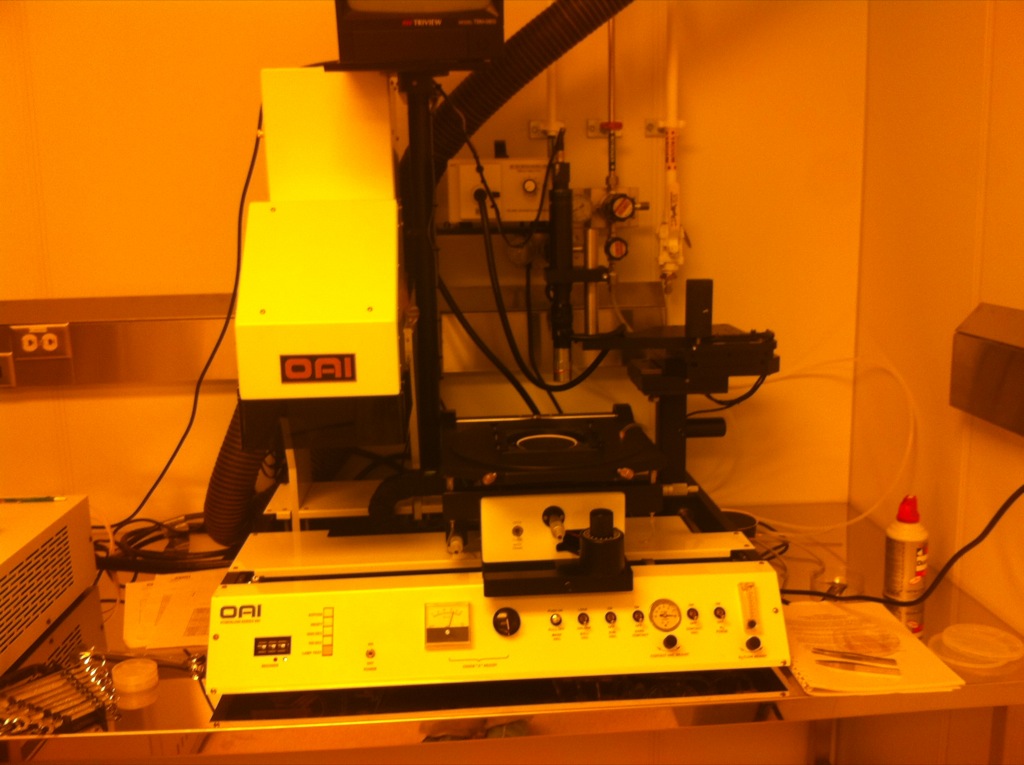
The exposure was done with the mask aligner. I did two exposures (one at 50s, one at 40s), and I believe I am probably over exposing. Using the vacuum chuck to adhere the sample and the mask at the same time works well (the mask extends further than the slide, so it has chuck exposure, not intended).Development was done with MF343 in a puddle for 45s. A final spin/rinse at 1500RPM for 30s, and then a hardbake at 150C for 5min.
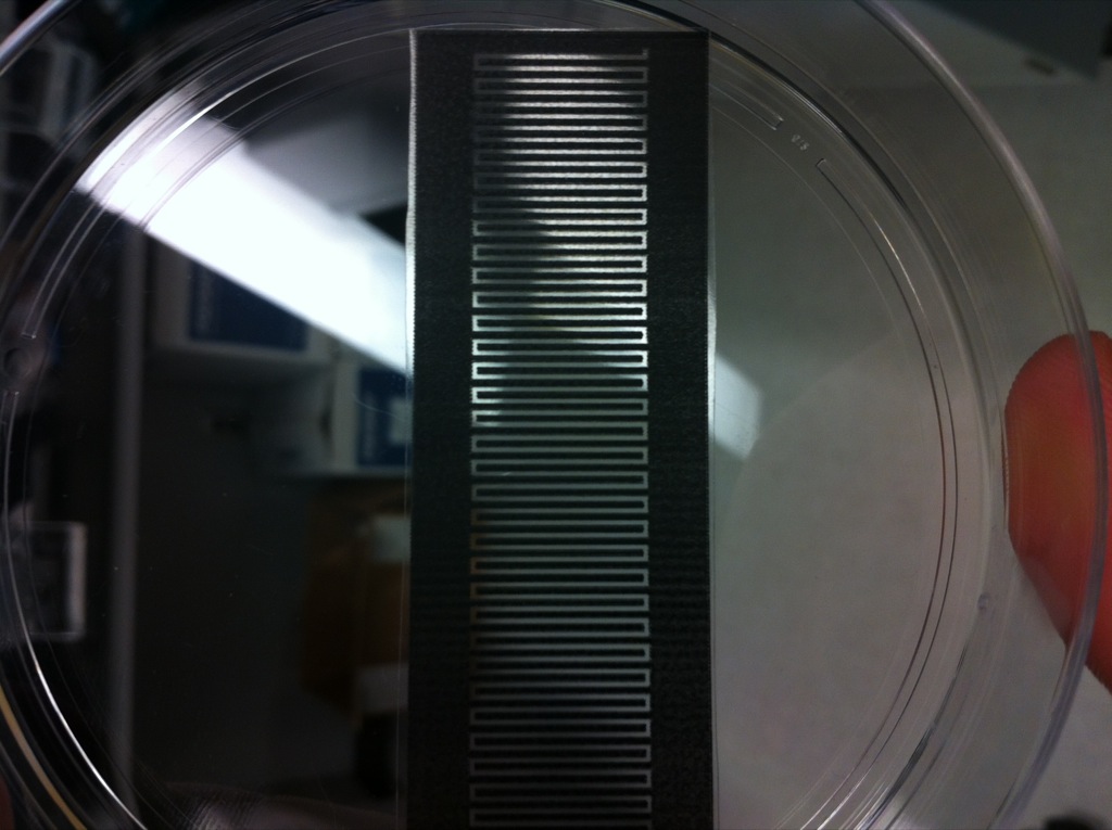
You can see that the actual pattern of the mask is reproduced reasonably well, including all the holes in the masked off area, and the line edge roughness geometry.

Wet Etch – I applied 0.5 mL of 12M HCL to the pattern for about 25 seconds. This was unintentional; I wanted to apply it for 15 seconds, but I had trouble handling the sample. I rinsed the sample in DI, then stripped the resist by puddling some acetone on the coverslip, wiping it off with a Kimwipe.
Results – Sure enough, there was electrical isolation from both sides (over 40 Mohms), but the resistance of the electrodes increased fairly significantly (one electrode had a total resistance of 25 kohms, the other about 8kohms), meaning that they are not useful for TEER measurements. For comparison, the electrodes created by scratching a dremel pattern into the microscope slides are about 600 ohms.
Things to improve
– Lower resistance of electrodes. Can do with thicker film, but transparency is reduced, or a better quality mask.
– Create higher fidelity mask. Use a different printer, maybe shop out to a 3rd party printer?
– Cleanliness. Coverslips could use a pirahnna clean before sputter. RIE is generally better for keeping surfaces clean.
*Need to replace videos with actual images…Exporter wasn’t working on DIC microscope.*
***UPDATE***:
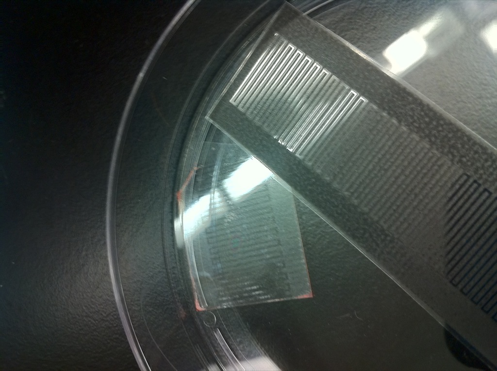
I used the Cornell-inspired recipe for ITO deposition, a higher fidelity mask, 15 sec exposure and got some much better results. The final diced form of the electrode produces a “pad-to-finger” resistance of 3kohms, which should be passable for my purposes (base line resistance assuming short between top and bottom electrodes is 6kohms. As said above, I am targeting sub 1kohm resistance per electrode. The line-edge roughness was dramatically improved from the first mask.
(pic)
(pic)
Need to work on my dicing technique some, doing it by hand currently
The overall working distance in the device is 600 microns with the incorporation of these coverslip electrodes. I still need to make a jig for the TEER readings.
Hi Greg, I might have some suggestions for ITO deposition. I have been using the PVD 75 for about a year now and copied the recipe they use at CNF for a similar tool. It’s called “Src3-*something*DC- Generic”. (I can’t remember exact name) It heats to 200C and uses 5% oxygen. It’s been the best compromise between resistivity and transparency that I’ve been able to get.
Also, I noticed yesterday that some of the copper back plate was showing on the ITO target, so your latest samples may have gotten some contamination. I replaced the target but the whole system looks ready for a thorough clean. I think I was the last person to do a clean, but I’m hoping Alex might take on that job.
If you want to discuss the recipes further, let me know and I can stop by your office. j.winans@rochester.edu
Cheers- Josh
Thanks Josh, that’s really helpful. I’ll check that out. Many thanks too for the contamination warning; I can pester Alex as well.
Do you have any idea what the thickness of the film in that recipe is? If it’s not in the title already…
The deposition rate has been close to 1nm/10s. I called it “Generic” because I wanted to change the parameters frequently. You need to open the recipe in the database and set the time you want. It should be the last box. I often deposit for 250 s and 450 s to get layers of 25 nm and 45 nm. Just let me know next time you plan to deposit and I can come down and discuss the other parameters. It would help me to hear what you’ve experienced thus far as well. Cheers- Josh