Nano-porous SiN Lift-off Update
Using the same successful procedure as the last lift-off attempt, another large piece of membrane lifted off. This came from the same wafer, but confirms that 30 minutes in BOE is sufficient to etch 25 nm of thermal oxide under the SU8 structure. Ideally this time can be reduced by means of a different sacrificial layer, since the SiN is also being attacked by the BOE at a rate of ~5A/min. This is a low rate, however given 40 nm of SiN, that will see BOE on both sides after approximately 1:45 minutes, this could mean anywhere from 15 to 30 nm of SiN is being etched.
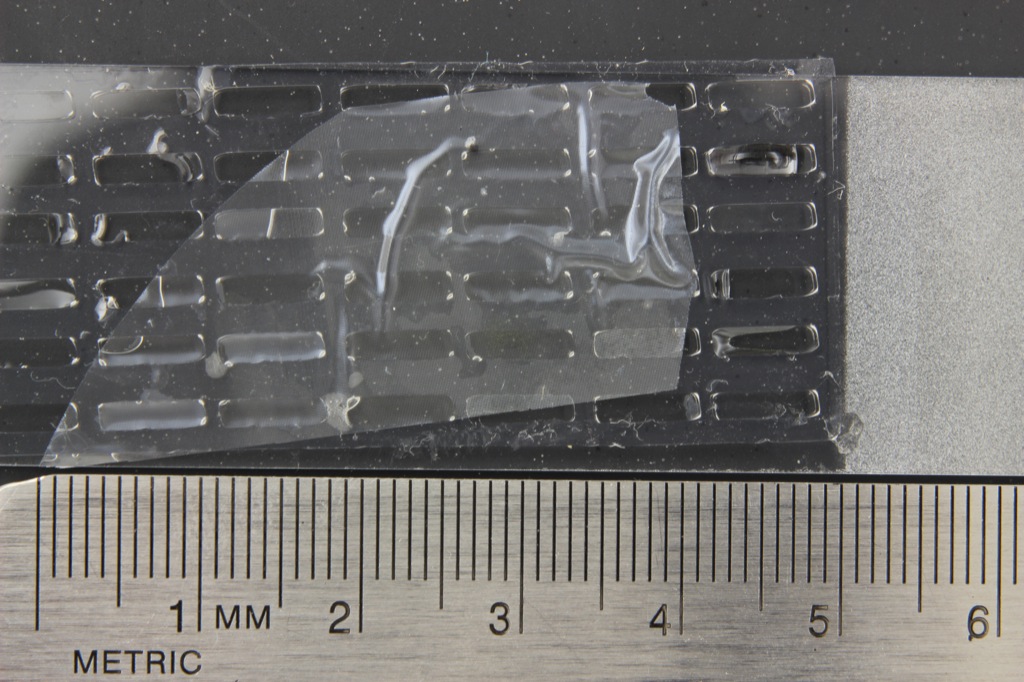
This video shows the beads coming to rest on the nano-porous membrane, the time lapse was set to 1 frame/sec, and beads were deposited 3 times in this video, every 100 (real time) seconds. As you can see in the image above, there are small ‘cells’ within the silicone sheet that the membrane rests on. After dispersing the beads, I checked the bottom of the entire cell and found no beads. This means a relatively large area of membrane has survived lift-off.
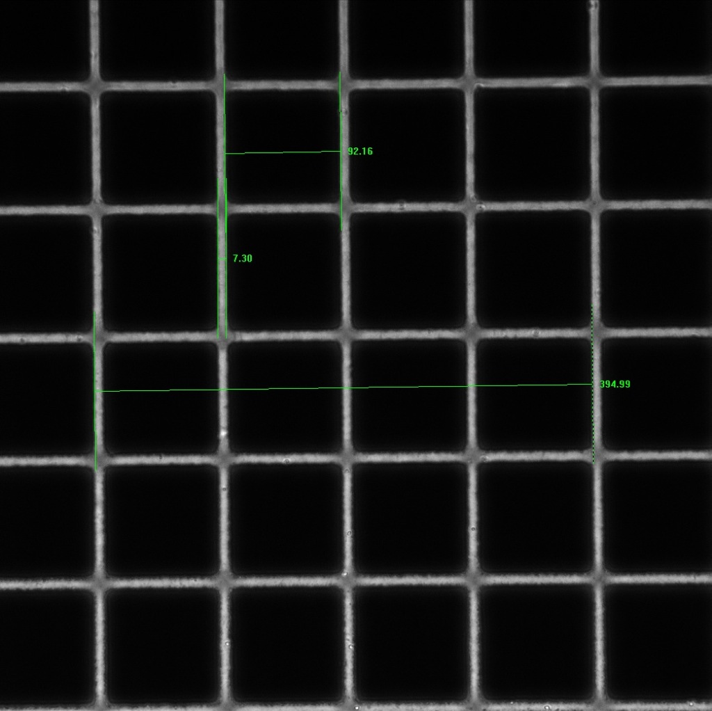
While designing the new masks for SU8, I discovered some discrepancies in the designs. The mask I used said 10 um lines and 50 um squares, the actual is 10um lines and 90um squares, this is a good sign, in that the SiN is robust enough for the larger windows. To verify the file vs. actual printed masks, I measured them after recalibrating the microscope. The results were 7.3 um lines and ~92 um squares. The printer used to make the mylar masks has a resolution of 3600 DPI, if you convert that to microns per dot, you get ~7um. The machine is incapable of reproducing the 10 um, so it shrunk it to 7 um and made the ‘inked’ or dark regions slightly larger to accommodate multiples of 7.
In the last post, it appeared that there was over-exposure of the SU8, but with a negative resist, the outcome of a high dose is different from positive resist. The SU8 profile is thickest around the perimeter of the wafer, and uniform and thinner in the middle. What was seen is likely due to the mask not contacting the center of the wafer, causing the light to scatter before entering the SU8. I discovered this by mistake when optimizing the exposure dose: to speed up the processing time testing silicon and SiN substrates, I placed both fragments under one mask, but the SiN substrate was 100 um thinner. The same SU8 structures developed in the SU8 on the thinner substrate as seen in the lift-off attempt, proving that there was some obstruction holding the mask off the surface.