AFM – wafer characterization
Chris gave me a few wafers to look at with AFM – an oxide sputtered in the recently cleaned chamber and VA Semiconductor wafers cleaned with “Normal Power” or “Full Power” Megasonics. I employed a couple of new “tricks” to help with the imaging this time. All of these scans were taken almost entirely in repulsive mode, which has been a challenge for me previously (the phase hopped briefly into attractive mode a couple of times, which you can see as lines running horizontally across the image).
First was a wafer that had 20nm oxide – this was sputtered after the chamber had been cleaned. There was one artifact right in the middle of the scan, unfortunately (I think it’s debris, not a particle). Other than that, the oxide looks very smooth (RMS roughness over 1umx1um was ~0.127 nm). This is a bit more smooth than 50nm AJA oxides as measured here.

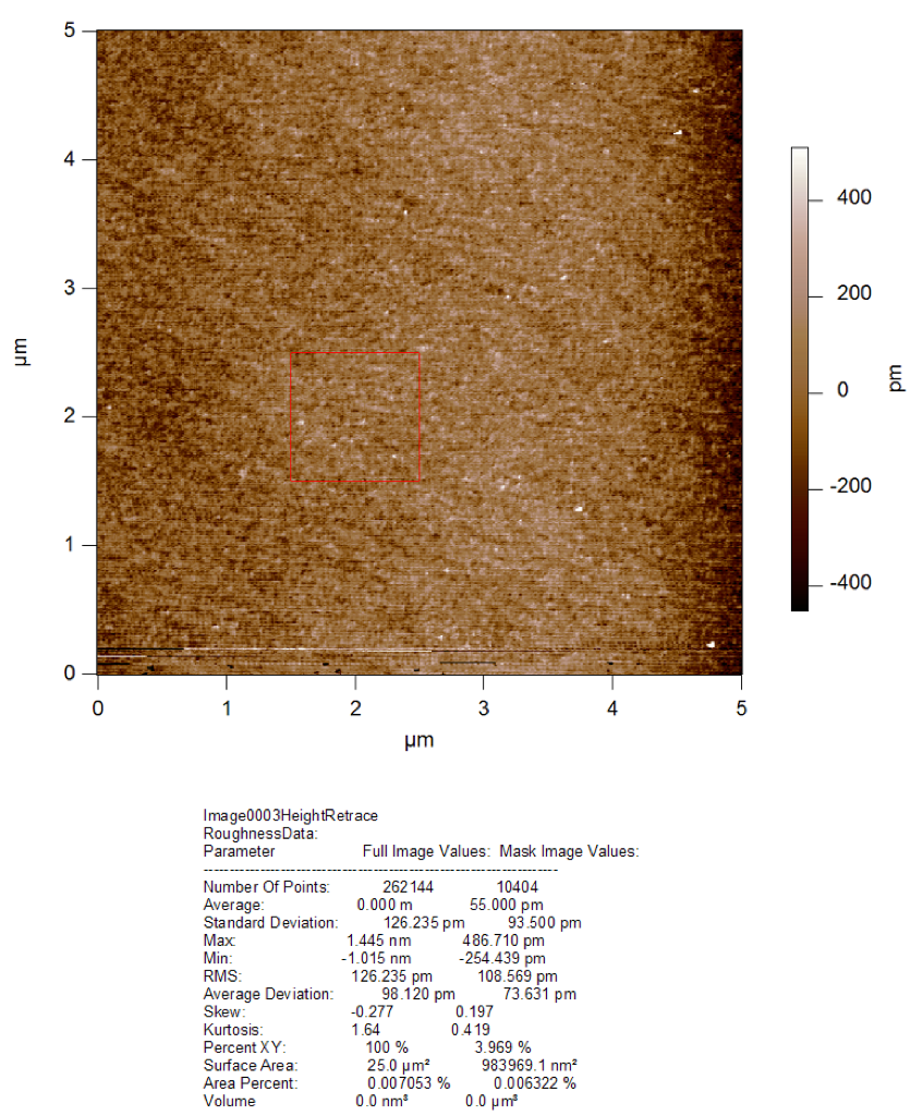
Here is the “Full Power” Megasonics-cleaned wafer. This is super smooth (RMS roughness over 1umx1um was ~.108 nm). This is in contrast with previous Megasonics cleaned wafers that showed particles (here and here). Perhaps “fullpower” is much more powerful than the 150W and 225W treatments from before.
Here is the “Normal Power” Megasonics-cleaned wafer. This is strikingly different from the Full Power wafer and for that matter, any other silicon wafer that I’ve AFM’d. The RMS roughness over 1umx1um is almost 0.4 nm. I’m not sure how to explain all of this surface topography – Chris suggested that these wafers may have been poorly polished. I did a scan of a different wafer from this batch and it looked the same.

Are we doing the ‘normal’ and ‘full power’ megasonics cleanings with our tool, or is this preparation done at VA semiconductor?
Still done @ VA semi