Record of light transmitting through the waveguide across the porous membrane
From the last post, I had successfully manufactured waveguide on top of our porous silicon nanomembrane chip. However, the proof that light can transmit through the waveguide was not accomplished until last week. The problems I was experiencing included insufficient thickness and wrong cladding layer refractive index. Thus, in order to prove that my waveguide is usable, I manufactured a waveguide with a larger thickness on top of cover glass pieces. All waveguides are S curve patterns. The core layer (waveguide) has a refractive index of 1.598 at 632.8nm wavelength. The cladding layer underneath the core layer is SiO2, which has a refractive index of 1.457 at 650nm wavelength. The upper cladding layer is air. The manufacture method is listed below:
1. Spin coat SU8 2002 with initiator at 1000rpm for 5s, 5000rpm for 30s and 1000rpm for 5s
2. Laser writer pattern the waveguide on top of the spin coated chip at exposure rate of 450 mj/cm^2
3. Post bake for 120s and Develop the patterned chip in SU8 developer for 60s
The first step is to manufacture and test the waveguide on top of a cover glass

Figure 1: Combined image of the waveguide on top of the cover glass when viewing from the top. The cover glass has a dimension of 22mm x 22mm. The dimension of the waveguide pattern is 15mm x 15mm.

Figure 2: Profilometer data of the waveguide on top of a cover glass. The thickness of the waveguide is approximately 2.9um. The width of the waveguide is approximately 9um.
The following setup was used for coupling light into the waveguide. The light source is a laser pointer with a wavelength of 650nm and a maximum power of 30mW. The microscope was used to monitor and record the appearance of the waveguide.
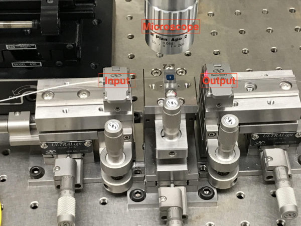
Figure 3: The setup system for light coupling.


Figure 4: Proof of light transmitting through the waveguide across the cover glass. Upper image corresponds to a smaller light input. Lower image corresponds to a larger light input. The last video illustrates the different appearances of the waveguide when turning the light source on and off.
Next step is to perform the same experiment on our porous SiO2 membrane chip.
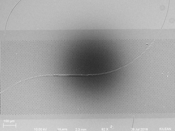
Figure 5: Image of the waveguide on top of porous SiO2 membrane
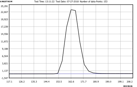
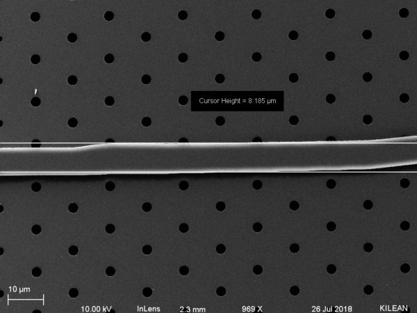
Figure 6: (upper) Profilometer data of the waveguide on top of porous SiO2 membrane chip. The thickness is around 2.3um and the width is around 8um. The variance of thickness is within about 0.5um. (lower) SEM examination of waveguide’s width.
In order to couple light into the waveguide, polishing step is necessary. The following two pictures demonstrate the different look of the waveguide before and after polishing.
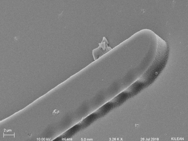
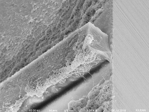
Figure 7: (upper) Before polishing (lower) After polishing. Those cotton-like impurities were adhered to the surface after polishing and could not be cleaned by IPA or water.
After the polishing step, we put our sample under the coupling setup shown before to prove that our waveguide is eligible for transmitting light across the porous membrane.

Figure 8: The image of how light coupling from the input fiber into the head of the waveguide (first half of the waveguide). There is a dim red curve at right, which is a leak of light from the waveguide, showing that there is light coupling into and propagating along the waveguide. The Media link on the right shows that how the leaked light shines when turning the light source on and off.
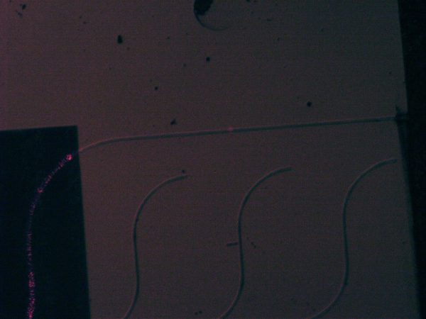

Figure 9: (Upper) second half of the waveguide before imageJ treatment. (Lower) second half of the waveguide after imageJ treatment.
We can clearly see that there is a small red spot after the red curve, which proves that light transmits through the waveguide across the membrane and diffracts by a defect on the waveguide. This also explains that why there was no light emission at the end of the waveguide. Because the last amount of light in the waveguide was diffracted by the defect.
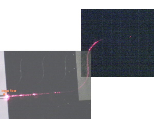
Figure 10: The combination of two images of the waveguide to give a better understanding of the whole pattern.
Even though we proved that light can transmit through the waveguide and across the membrane, the light outcome was too dim for detection. The next step will be characterizing and optimizing the waveguide, such as using modeling software to design the best size of the waveguide. Moreover, looking for a new way to polish the edge of the waveguide is necessary. Greg suggested that we can even vapor more glass onto the surface of the chip to increase the thickness of the glass cladding layer, though it might fill up the pores, we probably can find other ways to reopen the pores later. I also believe that a more powerful and stable laser source can increase the chance of detection of the light outcome.