Over the past year, our lab has been working in close collaboration with the Schwarz lab to design, develop, and manufacture microfluidic transwells for their P50 project. The project was initiated after the discovery of S. aureus migration through sub-micron canaliculi in vivo. To further explore the genes involved in this newly proposed mechanism of immune system evasion, the Schwarz group collaborated with our lab to hand build transwell devices that would allow them to mimic the confined geometries of the canaliculi. After the initial experiments involving strictly wt staph, candidate mutants were developed and are now in the process of being tested. In order to facilitate faster biological experiments, we contracted out Aline Inc, a microfluidic company based out of southern California, to build these transwell devices in large batches.
Design Stages
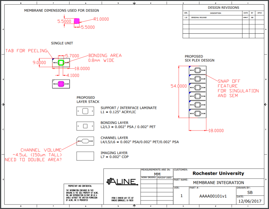
Figure 1. First formal Aline design. Bonding area was suited for three slot 0.5 um SiO2 format chips. The six-plex design was implemented to facilitate multiplexed experiments in an easy to handle format.Figure 2. Membrane failure during production highlighted a potential problem with the high number multiplexed design: if one membrane fails, the whole ‘device’ is not suitable for delivery. It was also harder to handle the six-plex devices then expected at this stage. For these reasons the design was changed to fit a three-plex need.Figure 3. High fluid resistance through the bottom channel, coupled with tiny access ports, made it near impossible to load the bottom channel of these devices. The bottom channel and access ports were both increased in size to adjust for these issues.
Figure 4. The discovery of potential leaks in the system lead to the shrinking of the sealing layer. This final design was easier to load through the bottom channel and was leak tested to confirm nice bonding.Figure 5. Leak testing confirmed firm bonding of the sealing layer to the Si chip.
Membrane Design
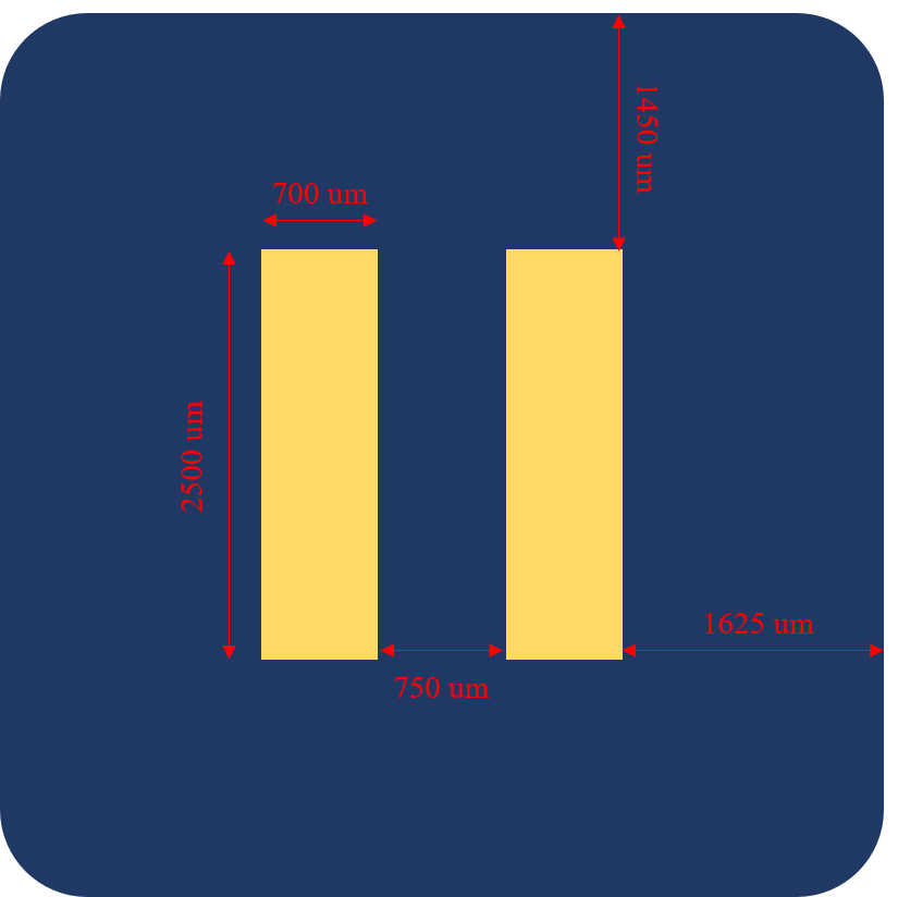
Due to concerns over the available three slot bonding area, two slot chips were designed. This design maintains high membrane area, while increasing bonding area.
Figure 6. 2-slot membrane format.Figure 7. Since completion of the design, we have been able to integrate a variety of membrane formats. The yields from these builds will help guide our future production runs.
This is the method Brian McIntyre developed for the recent URNano Microfluidics Workshop. Based on a polyaddition-based mechanism based on introducing amine groups onto the surface of one material and epoxy groups on another material and enabling the amine–epoxide polyaddition reaction at their closely contacted solid-to-solid interface to establish a covalent and permanent bonding presented in…
Last week, a RTP temperature series was performed on 15 nm Si membranes with 20 nm and 40 nm oxide layers. The purpose of this study was to 1. evaluate the effect of a thicker oxide on pinhole density and 2. identify a dependence of morphology on oxide thickness. Below are two graphs summarizing the…
These chips were 2.9 mm TEM grid with a single 25 um window. 20 nm thick NPN is covered with 100 nm TEOS with a 2 um opening to expose ~1000 pores. Wafer number 2176. Following are IV curve analyses for the above material as well as membranes treated with ALD alumina. These were measured…
Yesterday afternoon I made a new batch of 10:1 (base : curing agent) PDMS and put it in the oven at 80C for two hours to allow it to cure faster (compared to the three days it takes at room temperature). Once the PDMS was cured Henry used the UV Ozone system to again try…
This is my first attempt of depositing PEG using vapor deposition methods, in a controlled fashion. The stepwise procedure: Josh was extremely kind by providing me with a diced pncSi wafer [windowless]. He taught me how to do the buffered oxide etching to remove the native oxide from the surface. This step is just to…
Note: a postscript regarding an assay to determine the activity of our MMP-2/MMP-9 inhibitor was added to this post on June 14, 2021. Introduction The blood-brain barrier (BBB) plays an important role in maintaining brain chemistry by restricting the permeability of small molecules and cells. Inflammatory diseases may disrupt the BBB and promote the development…