Porous nanocrystalline germanium (pnc-Ge) membranes
Hello everyone! I’d like to show you some recent result about pnc-Ge membrane. We have been thinking to replace Si with Ge for a long time to see whether we can transfer pore formation to another materials other than silicon. In this post, I’m gonna show you some exciting pnc-Ge membrane images!
The fabrication process is similar to our previous one except free-standing SiN membranes were used as my deposition substrate. I deposited a 50nm thick SiN film on a patterned wafer and then etched through the Si substrate. After that I used these free-stand SiN membranes in a TEM grid pattern as the deposition substrate for the following deposition. Two different geometries have been tested, which are SiN/Ge/SiN (NGN) and SiN/Ge/SiO2 (NGO). The germanium films were kept at 25 nm and the top nitride/oxide layers at 30 nm. These grids were then rapid thermal annealed at different temperatures from 500C to 900C.
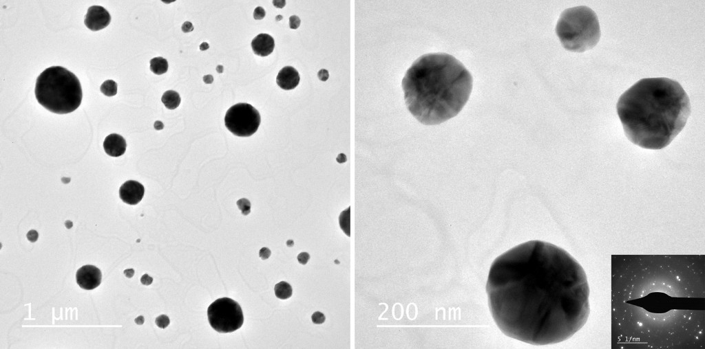
The first set of images are NGN and NGO samples annealed at 900C. It can be seen that Ge film agglomerated into islands during crystallization process, which is believed to undergo a melting-recrystallization process since the melting point of crystalline Ge is 938C (amorphous Ge has a lower melting point than crystalline Ge). The diffraction spots show the crystalline nature of these Ge islands.
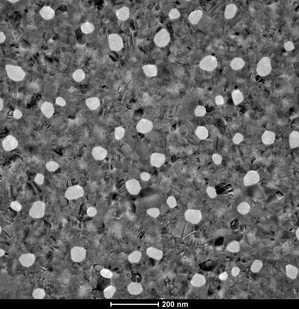
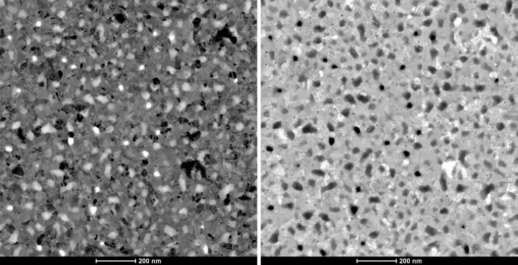
When the NGN and NGO sampled were annealed at 800C, the Ge films underwent a solid phase crystallization process where nanopores were formed! The followings are TEM and STEM images of NGN samples annealed at 800C. They clearly show pores in Ge films. The porosity is almost 10% with an average pore diameter of 53.4nm. This is the first time we demonstrate the pore formation in another material than Si!
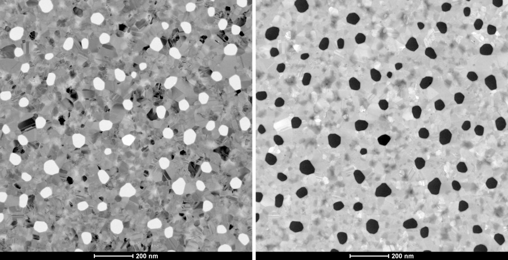
The next images are from NGO samples annealed at 800C. Nanopores are also formed in the Ge film after annealing. However, both the pore size and porosity is quite low compared to that of the NGN system. The porosity is around 1% with an average pore diameter of 22.7nm. Instead of through pores, voids/pits dominates the morphology of the Ge film. The pore characteristics difference between the NGN and NGO is similar to that of the Si system where the NSN yields the highest porosity and pore size.
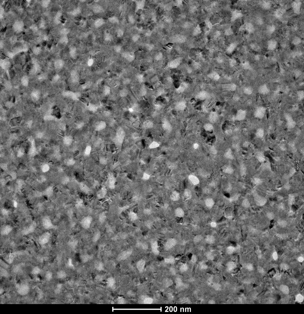
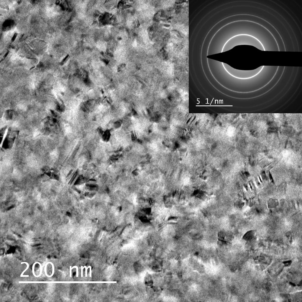
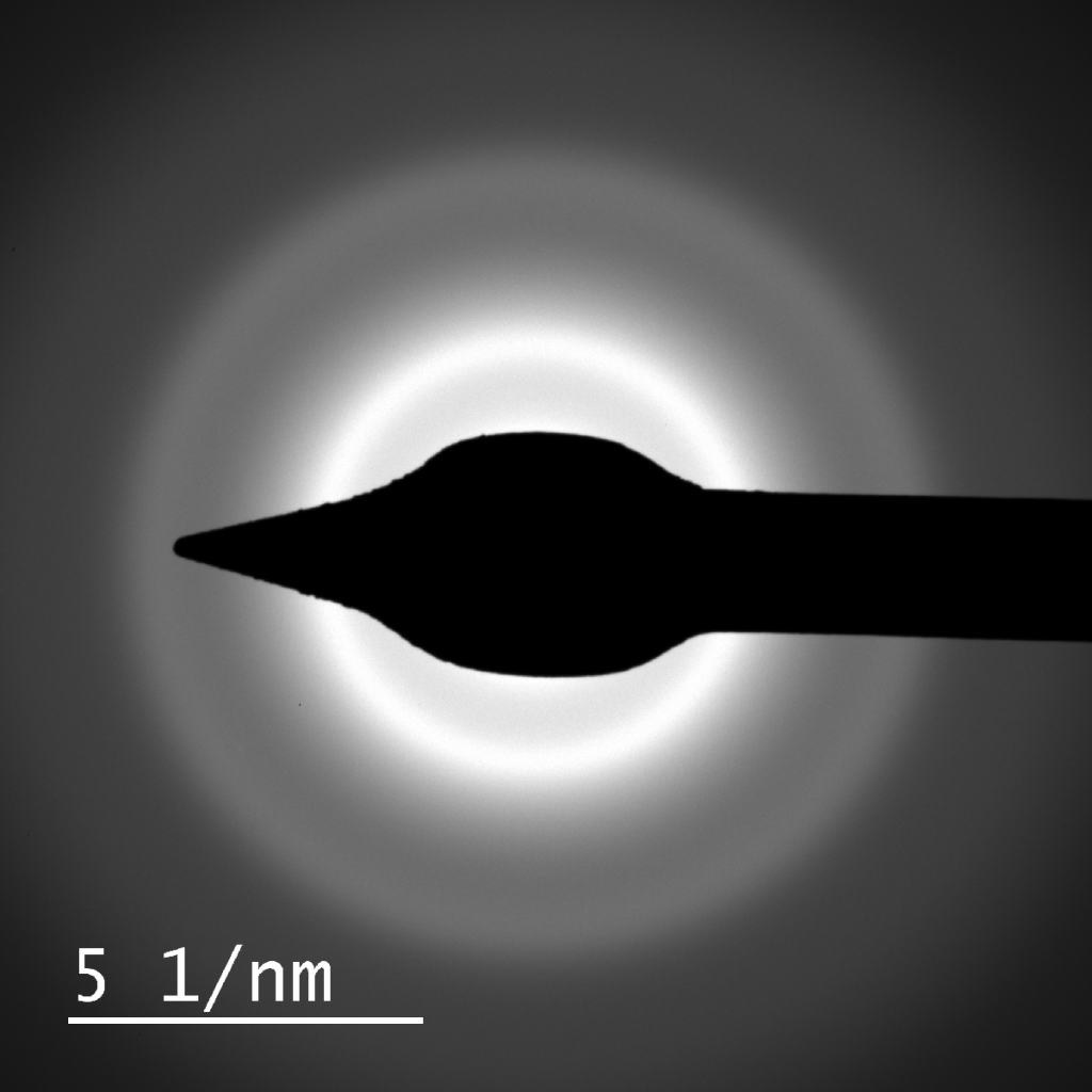
As the annealing temperature down to 700C, no obvious through pores can be observed in both the NGN and NGO systems. The diffraction ring shows the poly crystalline nature of the Ge film after annealing. Similar morphology was observed when both the NGN and NGO samples were annealed at 600C.
When the annealing temperature down to 500C, the diffraction result shows that the Ge film is still amorphous, which can be seen from the following images. It tells that 500C is not enough to crystallize the Ge film in both the NGN and NGO stacks.
In sum, this is our first time shown the pore formation in Ge material. It expands our current pnc membranes to the Ge system. This opens lots of research topics to further study the pnc-Ge membrane system!
Nice work Joe!
Can you comment on the yield and/or burst pressures for the pnc-Ge membranes?
Thanks- Josh
Thanks Josh. The deposition was done based on free-standing nitride membranes on a TEM grid pattern rather than on a silicon wafer. So I can’t comment on the yield at this point. But when I did the nitride/oxide stripping, it seemed that Ge film is quite strong, maybe even stronger than Si, because I didn’t see many broken membranes after the etch where it was at least 50% broken for Si membrane. So I guess the mechanical strength of the Ge membrane should be stronger than Si and the burst pressure should be higher.
This is really stunning to see. I can perceive no differences from pnc-Si other than the lower temperatures.
What is the next logical step along this line of work? Si-Ge alloys?
Yes, I think Si-Ge alloy could be the next step. However the chiller for the AJA is broken and we are working on this problem now, which may take some time. Meantime, I’m thinking doing some pore size control experiment at annealing temperature from 750C to 880C (maybe) to see whether we can get similar result of the pnc-Si annealing test.
Joe – Do you need help doing burst pressure? What are your thoughts on robustness of these membranes?
Hi Tom, I haven’t done wafer size fabrication on these pnc-Ge membranes since the pump broken of the AJA. I’ll let you know if I need help on the burst pressure test. Based on my observation, I think these pnc-Ge membranes have similar or even higher robustness than that of the pnc-Si membranes.