Microporous MgF2 Burst Pressure Fabrication and Results

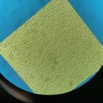
2. Yield after Etching
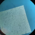
3. Yield after Evaporation
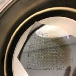
4. Yield after Dicing (least colorful)
| Window [mm] | Average | Std Dev | Count |
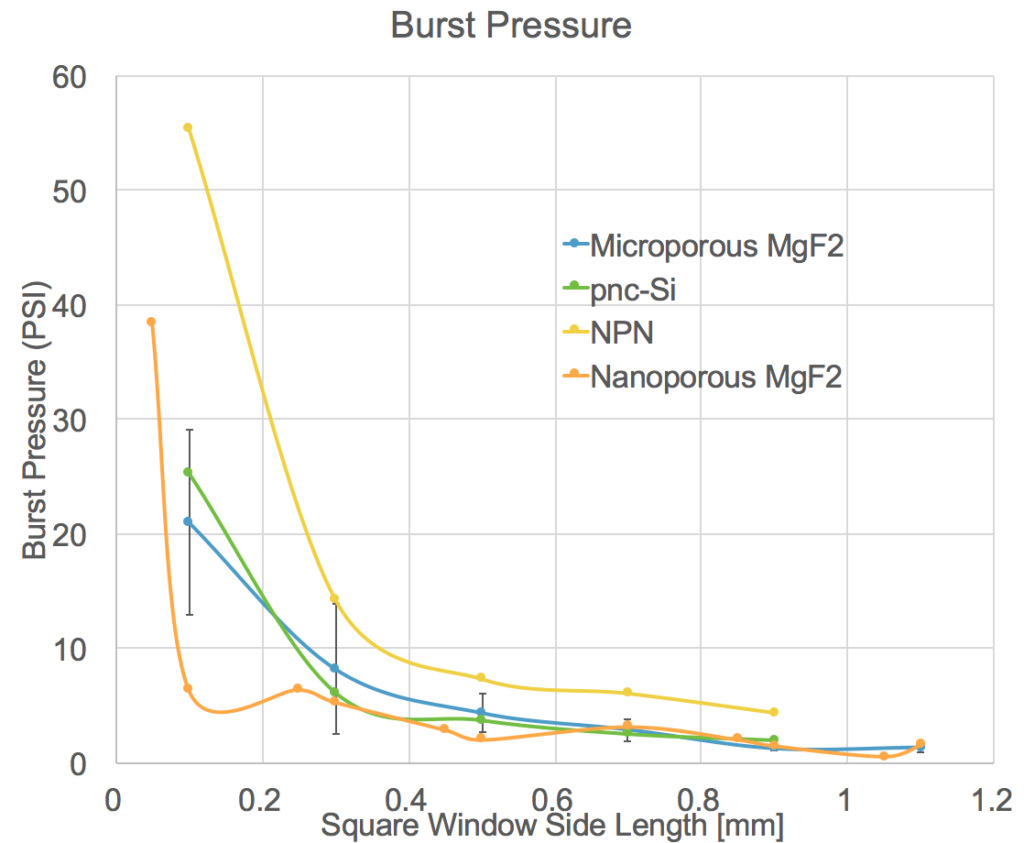
| 0.1 | 21.02 | 8.10 | 14 |
| 0.3 | 8.18 | 5.62 | 17 |
| 0.5 | 4.33 | 1.66 | 10 |
| 0.7 | 2.87 | 0.94 | 11 |
| 0.9 | 1.23 | 0.23 | 3 |
| 1.1 | 1.32 | 0.33 | 6 |
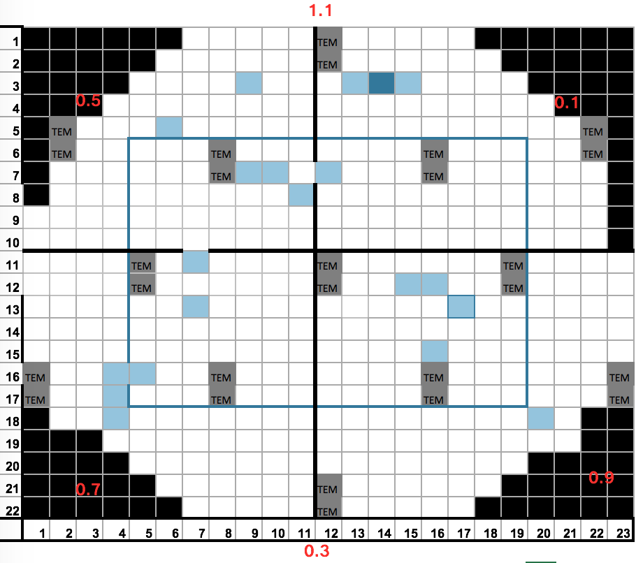
Our burst pressure wafer (Wafer #4632) has a number of window sizes (0.1, 0.3, 0.5, 0.7, 0.9, 1.1 mm square windows) and varying porosity (low = edge, high = center). I was targeting 200 nm thick MgF2.
I began by splitting the wafer into 4 pieces (quads) so that they would coat evenly on our evaporator.

Each quad had a separate deposition, and the film thicknesses (measured with profilometer) varied a little:
Deposition settings
- 6KVOxide Recipe
- 1 mA beam current
- 2-4 Angstroms/sec
- 200 C
- Platen Rotation on
- sub 5-e5 torr base vacuum
| Top Left (1) | 165 nm |
| Top Right (3) | 174 nm |
| Bottom Right (4) | 173 nm |
| Bottom Left (2) | 210 nm |
These chips are then ready to be etched
Etching Settings
- 2.5 mTorr Oxygen (8.9 Setpoint)
- 47.5 mTorr CHF3 (26.9 Setpoint)
- 110/10 W Fwd/Ref
- ~100 mTorr Etching Pressure
- 5.5e-5 torr base pressure
- Samples face down on carrier wafer
- 120 second etching time
Each Quad was etched with these settings. The chamber was first cleaned with a 5 min, 200 W, 100 mTorr Argon plasma, then seasoned with the etch recipe for 5 minutes.

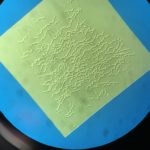
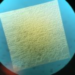
Inspection of the chips revealed some interesting cracking structure. These were seen across the whole wafer, revealing a difference between central and edge chips (porosity difference). Maybe this explains the noticeably lower yield in the central region?

Overall Yield was 51%, where 89% made it through evaporation and 57% made it through the etch. As with the first burst pressure wafer, there was strong dependance on window size, but also the higher porosity material was less likely to survive (about 2-3x poorer yield).
This compares very favorably to the thinner 50 nm nanoporous process which had 22% yield of mostly smaller windows.
| Window | Edge Chips Start | Edge chips after Evap | Edge chips after Etch | Yield After Evap | Yield After Etch | Etch Process Yield |
| 0.1mm | 30 | 30 | 26 | 100% | 87% | 87% |
| 0.3 | 39 | 39 | 38 | 100% | 97% | 97% |
| 0.5 | 30 | 29 | 24 | 97% | 80% | 83% |
| 0.7 | 32 | 29 | 23 | 91% | 72% | 79% |
| 0.9 | 31 | 9 | 3 | 29% | 10% | 33% |
| 1.1 | 36 | 31 | 9 | 86% | 25% | 29% |
| Sum | 198 | 167 | 123 | 84% | 62% | 74% |
| Window | Center Chips Start | Center Chips after Evap | Center chips after Etch | Yield After Evap | Yield After Etch | Etch Process Yield |
| 0.1 | 35 | 35 | 30 | 100% | 86% | 86% |
| 0.3 | 28 | 28 | 17 | 100% | 61% | 61% |
| 0.5 | 36 | 35 | 17 | 97% | 47% | 49% |
| 0.7 | 34 | 31 | 9 | 91% | 26% | 29% |
| 0.9 | 34 | 31 | 2 | 91% | 6% | 6% |
| 1.1 | 28 | 24 | 2 | 86% | 7% | 8% |
| Sum | 195 | 184 | 77 | 94% | 39% | 42% |
| Total Chips | Chips Left after Evap | Chips Left after Etch | Yield after Evap | Yield after Etch | Etch Process Yield | |
| Total Sum | 393 | 351 | 200 | 89% | 51% | 57% |
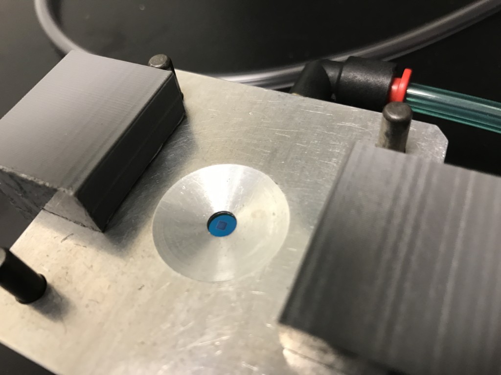
After this quantification, we had to see how strong the membranes actually were. The chips were clamped into a burst pressure rig, and then destroyed using a slow nitrogen flow, ramped up by hand (0.2 PSI/sec).

I tabulated the burst pressures for each porosity. There were no significant differences (t-test, 2-tails, 95% confidence level, unequal variances).
| Center | ||||||
| Window [mm] | 0.1 | 0.3 | 0.5 | 0.7 | 0.9 | 1.1 |
| Average | 21.1 | 7.2 | 3.7 | 3.0 | 1.1 | 1.0 |
| Std. Dev | 10.3 | 4.1 | 1.5 | 1.2 | 0.4 | |
| n | 9 | 5 | 5 | 7 | 1 | 2 |
| p-value (Different?) | 0.951 | 0.587 | 0.289 | 0.494 | 0.122 |
| Edge | ||||||
| Window [mm] | 0.1 | 0.3 | 0.5 | 0.7 | 0.9 | 1.1 |
| Average | 20.9 | 8.6 | 4.9 | 2.7 | 1.3 | 2.1 |
| Std. Dev | 0.8 | 6.3 | 1.8 | 0.4 | 0.3 | 1.2 |
| n | 5 | 12 | 5 | 4 | 2 | 5 |
Finally, combining all chips:
| Window [mm] | Average | Std Dev | Count |
| 0.1 | 21.02 | 8.10 | 14 |
| 0.3 | 8.18 | 5.62 | 17 |
| 0.5 | 4.33 | 1.66 | 10 |
| 0.7 | 2.87 | 0.94 | 11 |
| 0.9 | 1.23 | 0.23 | 3 |
| 1.1 | 1.32 | 0.33 | 6 |