700nm~1um thickness photoresist gasket
There are four main challenges for making such a thin photoresist gasket on a little chip.
Q1: How can I get under 1um thickness photoresist gasket?
Q2: Is the adhesion of photoresist gasket strong enough for further usage?
Q3: How can I write the pattern onto the gasket that will have the center window open?
Q4: How can I make sure that no photoresist will clog in the pores?
Q1: we must make a photoresist layer that is thin enough to reach our requirement. I use SU8-2002 and spin coat it on a sample chip.
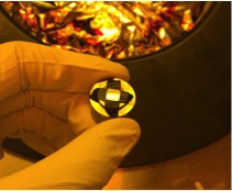

Image1-1(up): I use double-sided tapes to hold the chip because the chip is too small to be held by the vacuum.
Image1-2(down): The chip after spin coating. This one is successful on the uniformity.
The spinning setting is 500rpm for 5 seconds; 800rpm for 10 seconds (These two steps are aiming for more uniform surface); 9000rpm for 60 seconds (This step is to thinner the layer).
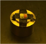
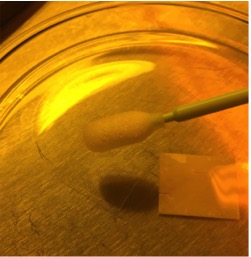
Image2: I wiped off half of the gasket in order to measure the thickness of the photoresist gasket.
The profile of the surface is at below:

Image3: Part of the surface profile. The peak is the accumulation that happened when I wiped off half of the gasket. The thickness stables at around 900nm. (10000 angstrom = 1 micron)

Image4: This is a very beautiful and flat graph. We can clearly see that the thickness nearly stables around 700nm. (10000 angstrom = 1 micron)
Q2: Then I proceed to next question, which is to test the adhesion of this thin photoresist gasket. The reason I choose SU8 as photoresist is that it has a good adhesion in most of time.
The procedure is:
Spin coat the chip; soft bake at 95 degree C for 1 minute;
Put HMDS (adhesion promotor) on the glass plate.
Bring the chip and sample glass together; soft bake at 95 degree C for 90 seconds;
hard bake at 185 degree C for 20 minutes.
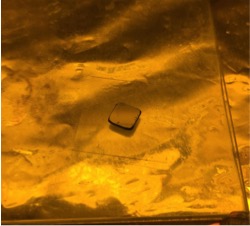
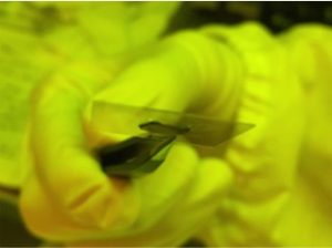
The adhesion is not as strong as PDMS, but it is strong enough to stay together if you don’t mean to separate them. Here is a pictures of one sample (this is not the perfect one):

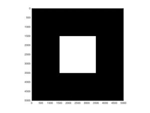
Q3: There is a new laser writer in our clean room that can write any pattern on any photoresist layers. So, I am trying to write an open window at the center of chip. Like the picture illustrated below:
I’ll use laser writer to expose the blue part, then bake it at 95 degree C for 20 minutes. After that I will use SU8 developer to wash away the white part (unexposed). However, SU8 has a very low absorption rate for the laser writer we have. After failing several times, I finally successfully pattern the chip like the picture showing below:
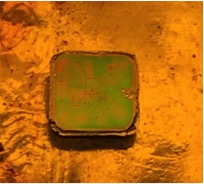
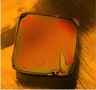
Image5: Sample chips after post-exposure bake, before going through developer. You can clearly see the square at the center of the chip.
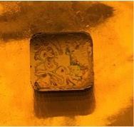
Image6: Sample chip after develop. The center square is clean now.
Then I continue to test the adhesion of this photoresist gasket that has been exposed. It is the same procedure as Q2 illustrates.

Image7: Exposed chip bonded stably with the glass plate. This means the exposure step won’t affect the adhesion of the photoresist gasket.
Q4: Not done yet.
Summary:
Now we have approved that making a 700nm thickness photoresist gasket is possible. However, the laser beam from the laser writer I am using is the inappropriate one for exposing SU8. The absorption rate is too low to expose the whole surface completely and nicely. Since we don’t have a chance to change a new laser beam, I am looking for a new photoresist material to replace SU8. I will continue working on this project this fall semester. And I believe finding a substitute for SU8 is not as hard as the progress I’ve made until now.
Great work. Brian says there is an additive we can use that will make the SU8 more responsive to the laser line of our mask writer. Hopefully this doesn’t negatively impact the adhesion or ability to spin under 1 µm.