Membrane thickness series
A few weeks ago, we made wafers with three different silicon thicknesses: 15 nm, 30 nm, and 50 nm. The goal was to see how pore morphology changes with increasing thickness. The films were deposited at 450 C with a 25 W substrate bias. The annealing temperature was 800 C in the susceptor. Note that the oxide was contaminated with copper which can be seen in the micrographs.
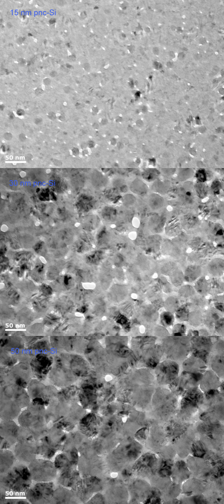
The 15 nm film looks strange. The darker spots might be contamination. The pores do not look circular (as they should be with this thermal treatment). At 30 nm, larger pores open, but there is a grain structure in the background. Perhaps the contamination is causing the silicon to nucleate preferentially. The pores seem to form between these boundaries. At 50 nm, the density of pores drop.
Here’s a comparision of a 30 nm film with two RTP temperatures.
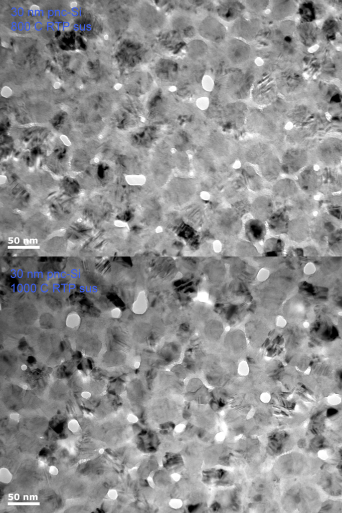
As expected, the higher temperature anneal opened more pores. Unfortunately, these wafers had a high density of pinholes. There was, however, a trend of higher (relative) burst pressure with increasing thickness.
A repeat of this experiment will need to be done once there is room in the experimental queue.
I learned how to use the EDAX on the SEM recently. It can pick up atomic signatures, so if we want to confirm that it’s copper, I should be able to do it on the SEM. I heard that the EDAX on the TEM at the Med Center is finicky.
If you have time, that would be awesome.
Typically EDX in an SEM requires quite a bit of the material that you are looking for. I have a feeling that it will be very difficult to see anything beyond Si and O, but it is certainly worth a try. Thanks!
I’m not sure about sensitivities. I can move the beam spot around on the film to try to pick up non Si/O peaks. I’ll talk to Brian in the next couple of days and try to get on it during “spring break”.