Imaging SI atoms at UR
Here’s a cropped image from a recent TEM pic that Brian McIntyre took of our material for SiMPore (15 nm thickness, not sure what wafer). This particular feature caught my eye because the crystal is perfectly aligned so we are looking at individual atomic columns of Si, instead of the typical crystal planes. These happen to be <110> oriented, which is more impressive, given the 1.9A spacing. The now “standard” <111> planes that we see everywhere are 3.1A spacing. The verdict is still out on whether there is any preferential alignment of the nanocrystals in our films, but at 15nm thickness, it seems fairly random.
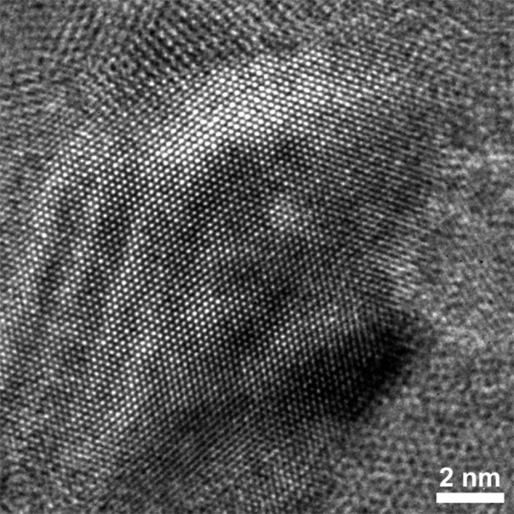
Anyway, it appears that we now have on-campus access to very powerful EM capability that will hopefully allow us to better understand our material and other materials that we can deposit on it.
wow, these are really cool pictures! It still amazes me that so much of the material reveals either atoms or crystal planes- if the orientations were truly random, I would epect that only a very small percentage of the membrane would show planes or atoms. I think this will hold true even though our films are thin- they are not thin enough to allow Bragg diffraction when the crystal are only slightly off.