AFM-newer material and high "magnification"
Earlier this week, Maryna and I did some AFM of her samples. She vapor-deposited parylene on the well-side of pnc-Si and was interested in whether/how well that polymer got through the pores. We got some really interesting-looking scans, but I’ll let her post those images.
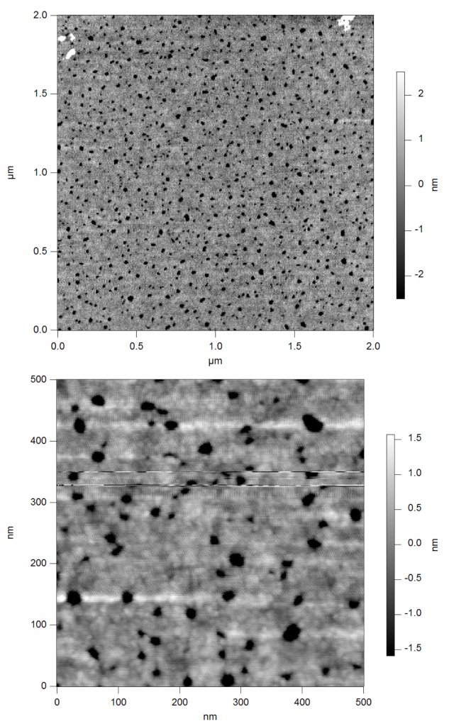
As controls, we looked at clean chips from the same wafer, SC115. These are areas of supported pnc-Si, not the free-standing window. I wanted to include them since they’re nice images, and I haven’t looked at AJA material with the AFM until now (last one was w673). Note that there are no “bubbles” as claimed by the Solver-Next AFM people. Also, the 500nmx500nm scan was the highest “magnification” scan I’ve been able to get without repulsive/attractive phase issue. Unfortunately, you can see where I bumped into the AFM cage by accident between 300-400nm in y-axis.