Diffusion Separations w/ 670, 673
Wafers 670 and 673 were made to have different cutoffs. I set up diffusion experiments with two chips from each wafer using protein standards. However after removing samples after 24 hours I noticed that both chips from w670 had fully discolored and the chips from w673 seem to have partially discolored. In all three cases it appeared that the active membrane had broken or dissolved. Here are images after collection:
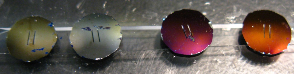
(2x 670 on left, 2x 673 on right)
Even though I was certain the experiments had been compromised, I still ran the gels (mostly to get some practice in since I haven’t done a gel in a while). As I thought, there were no cutoffs at all and all proteins were seen on both sides of the membrane.
What is different with these chips? The membrane side was exposed to PBS (~100mM salts) for 24 hours and the well was filled with ~1mg/mL protein. This is the same as all of my previous experiments.
Results from pressurized tests are pending gels. The membranes were strong enough to hold up at 2psi in pressure cell.
UPDATE:
Once before I had seen discoloration during a diffusion experiment. I write on 5/14/07:
“both membranes from w265 turned colors where they touched the PBS reservoir, ~ ocher color”
This was concomitant with Joe Fantuzzo’s experiments so I guessed that something similar was happening. Also instead of applying protein standards to the top, I used a 1 mg/mL b2-microglobulin and albumin mixture.
You could try doing some type of annealing treatment with and without ozone treatment, like we have tried with the cell culture setup.
Has anyone done discoloration experiments on the old material from the Nature paper? I have been concerned for a while that the same impurities that we have been working to eliminate to give us better control over pore size, have actually been helping our chemical stability. We know that SiO2 is more chemically stable than Si, so this is pretty obvious.
Anyway, I would start by seeing if there is any really old material left around, and see if we see the same problem. Joe may have done this already, so if anyone has time to look at his data, there may be some clues there.
Also, you could try dropping the pH of your solutions or pre-adsorbing something sticky like BSA at high concentration (maybe 10-100 mg/mL). It’s widely available at 200 mg/mL, but that’s pretty thick stuff.
Also, I don’t know how the silanization work has been going, but this is the best solution to this problem. Given all the fabrication delays that we have encountered, there has been plenty of time to develop a workable silanization protocol, but I guess we decided that the RTP treatment was fine. Did we abandon the chemical functionalization approach entirely? Seems like a PEG-silane or carboxl-terminated silane would solve this problem. If we can keep oxygen-containing ions off of the Si surface, the dissolution should go away.
The infotonics center has a vapor silanization tool that may also work for you. It’s not as nice as the one that we are planning to buy, but it may help bridge the gap. I have no idea how they work with universities on a toll-specific issue, but Jim and Philippe may know. Alternatively, maybe Cornell has a tool that you could use to coat your samples. There’s nothing that I know of at UR or RIT, other than the RTP treatment (maybe w/ a little O2?) or PVD (Physical Vapor Deposition – evap, sputter, etc.)
We also have the carbonization process in the RTP to develop that may resolve this issue. if someone wants to help drive this project, Dave and I could assist, but we don’t have time right now to make this a full-time effort.
Anyway – there’s lots of solutions – let me know if I can help!
Huh?
Why are we brainstorming surface modifications to allow us to look at overnight protein diffusion in PBS on the benchtop? We’ve done this type of experiment 300 times and 2 times it has given discoloration!
We should be trying to figure out what is unique about these particular membranes. Again we are 2 good membranes with different cut-offs away from finishing Jess’ work on movable cut-offs. Publications are vital and our absolute top priority. Lets stay focused! These membranes had the right stuff except for this unfortunate result.
We’ve often speculated that some etchant failed to be cleaned out when thinking about reasons for discoloration. We’ve ruled this out as the reason for all discoloration but it certainly could affect us now and then. There are more and more hands involved in the preparation of membranes. What is the history here and what might have been done differently? Dave can you comment please?
In the meantime we need to test everything that is being produced today for stability in PBS. The most reasonable assumption to make is that this is an anomaly that we need to learn about so we can avoid it in the future.
Here is a link to all of Joe’s discoloration experiments. All data was for w124. He never saw discoloration this fast in PBS.
The current material is purer Si than anything that Joe apparently worked with. I had thought that he may have used wafers left from the Nature publication, but if w124 is it, I guess not. Anyway, what you are seeing in these samples is probably what the Nature material would have done – that’s why I asked if he ever worked with the Nature stuff.
This purer material is what has allowed us to control the pore size again. Unfortunately, we really can’t “dirty-up” the machine again to go back. Even if we go back, we can’t control pore size. I’m not sure how to proceed, other than to try the approaches that I outlined. Some of them are easy, so why not try, as there is little that we can do from the fab side of things….
I refuse to accept this as a reasonable conclusion given an uncontrolled (unintentional even) study.
Can someone check if the AJA material w613(?) discolors overnight in PBS? That should be pretty pure too, right? Are there other pure (recent) wafers to test?
I’m not easily discouraged, but frankly if we need to surface treat membranes to do the simplest of experiments, I’m discouraged.
Note that none of the wafer summaries on this blog say if the material was produced with the ‘re-built’ deposition system or not. We need material just before and just after rebuild please.
Was wafer 677 deposited after wafer 670 and 673? If so, Jess did this protein separation experiment without discoloration. Rachel also worked with the same material overnight in PBS without trouble.
Jess should also be thinking about how her solutions might have been different. Retesting these same wafers in fresh PBS would be worthwhile.
As Chris mentioned, there seems to be a trade-off now between improved chemical resistance (impurities in the film) and better looking/purer material (rounder pores, less background, pore size control). I would argue that it’s more important to create purer material which can then be treated post-production to improve chemical stability (silanization, oxidation, carbonization etc…)
The AJA tool is very close to being operational and I estimate that we’ll be able to churn out a test wafer with the membrane stack by the end of this week. The films will most likely be non-optimized but it should give us a point of comparison.
We’ve done this for years now. Much of that time we had stable material for protein studies AND different pore sizes. The idea that everything we’ve known is for ‘contaminated’ material is flat out maddening. If it is a matter of raising the base pressure during deposition to make useful stuff – I’m for that.
In the meantime, what # wafers are post-rebuild please? I really want to see this result in a controlled study.
Checking out the AJA wafer is a good idea, but it seems like this was done, at least for the other solutions, so maybe someone can comment. This wafer also had 2X thicker membranes, so if it is not at least 2X more chemical resistant, it is likely a less chemically-stable material.
It is odd that there is such a difference in the 900C and 1000C anneals in the picture in this post. I also don’t know why there would be variability within each condition. Surprisingly, the color change is also much more uniform than we have been seeing, which is strange. Also, I don’t remember seeing the red/orange colors before – are they really new or just how the pics were taken?
We should examine these films with EM and AFM to better understand what is going on. We need to figure out if the films are getting more rough or if the pores are growing during the process. We can also try other deposition conditions to try and balance this effect, but if silicon is the problem, our options are limited. Understanding the rate of color change would be helpful – my guess is that the membranes are stable for a few hours, so maybe experiments can be modified to work within this time frame for now.
RTP and ozone treatments may also be more effective on this material than the older stuff. We may even be able to grow a continuous thin oxide that’s very effective – we just don’t know at this point.
From everything that we’ve discussed in journal club and from presentations and literature, I have the impression that silicon dissolves in physiological fluids, whereas SiO2 and most polymers do not. Apparently, the current membranes do not have much of a native oxide, so bolstering this oxide seems like the best short-term approach. However, projects that look more long term are also critical.
Here’s a link to Karl’s post on discoloration of the AJA sample. Without RTP treatment, it looks like discoloration rate is similar to the current material. Notice Chris’ comment on the uniformity of discoloration of the AJA material. Could this be a consequence of purer material? It makes sense that the impurities in the film would localize discoloration, right?
I’m not great at taking this discoloration pics (maybe someone can show me the method they use), but I think this is a reasonable depiction of the colors I am seeing.
These new wafers are also slightly on the purple side to start with, when compared to the normal dark blue starting point.
With respect to taking pictures of discolored membranes, I think it would be worth investing in a light tent (box and light). The diffuse lighting should give a more consistent portrayal of color.
Regarding lighting – be careful. We need specular, and not necessarily diffuse illumination. A light-tent or box is good if there is an angle at which you can capture the reflection of a pure white background/illuminator. Tom has some experience with this from the UR photographer who took some early pictures of our material.
Interesting. I can add a few things. First, we looked at silanization and discoloration and it didn’t seem to help. Dave linked to the post, but those experiments were done in DMEM, not PBS. DMEM discolors much faster than PBS.
Dave – Can you email me some of those papers you mentioned about porous silicon degrading in physio. fluids?
Jess’s pictures look fine, I think. We have no real standard protocol for discoloration pictures. Basically, we put the chips on a white background and underneath a fluorescent lightbulb and take a picture with the lightbulb reflection on the chips.
I’ve found that in the blue chips, the very first stage of discoloration is a purplish color. This makes sense if we are saying that discoloration is a result of thinning the Si from 15nm->13nm->something lower.
I was gone for a couple days but am ready to do discoloration tests if necessary. I’ll start one with w670 and w673 tomorrow.
Barrett – please compare older material to w670, w673 and any other post-rebuild material you can find. Dave explains that post-rebuild is anything under wafer summaries after 9/27. Note that the wafer numbers and production dates don’t correspond lately for some reason.