Production from 2.14.2008
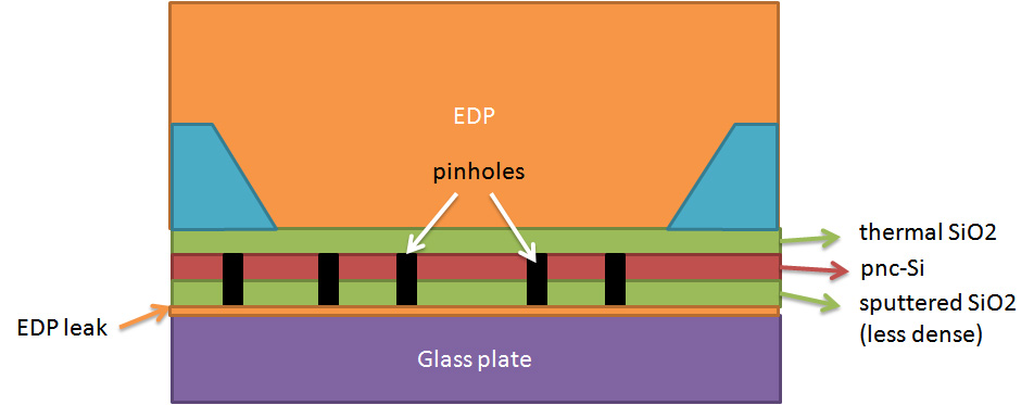
Production was scarce last week because we ran into some problems with our patterning/etch process. The first two wafers I attempted to etch did not react with the EDP because there was a thicker than normal layer of oxide remaining after our lithography step which prevented the EDP from attacking the underlying bulk silicon. We’ve resolved the issue, and have successfully etched one wafer (403). However, this wafer is completely covered with pinholes (images below).
JP has developed a new process at RIT to help cut down on surface contaminants by growing a 200 A thermal oxide on bare wafer as soon as it comes out of the box. While in the past we’ve stripped this thermal oxide during the patterning step, we now leave the thermal oxide on the wafer and deposit a second layer of oxide (TEOS) on the backside that is subsequently patterned. This gives us the advantage of never having to expose the bare silicon frontside. JP will post a detailed process flow soon.
During the deposition step, I can now directly sputter amorphous silicon without an initial layer of SiO2. The thermal oxide layer is much more robust (dense) than the sputtered SiO2. Unfortunately, we still rely on a sputtered silicon dioxide film as our “capping” film over the amorphous silicon. Any EDP that manages to get in between the frontside of the wafer and floor of the etch cell causes problems because it will eventually penetrate the sputtered SiO2 layer and start attacking the pnc-Si film. This is what we think is causing the high density of pinholes.
Images from wafer 403
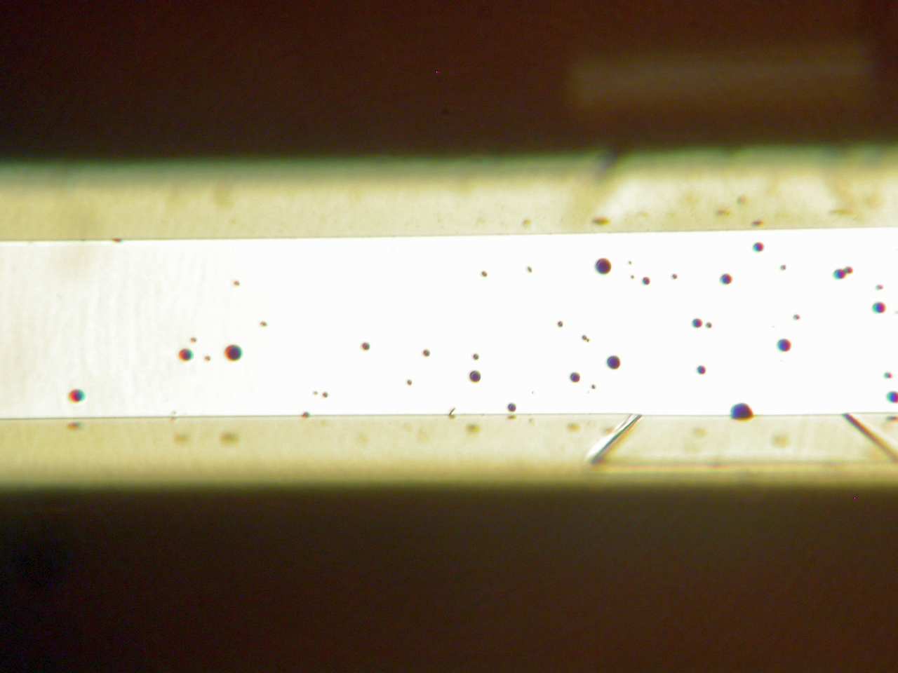 looking down at the well-side
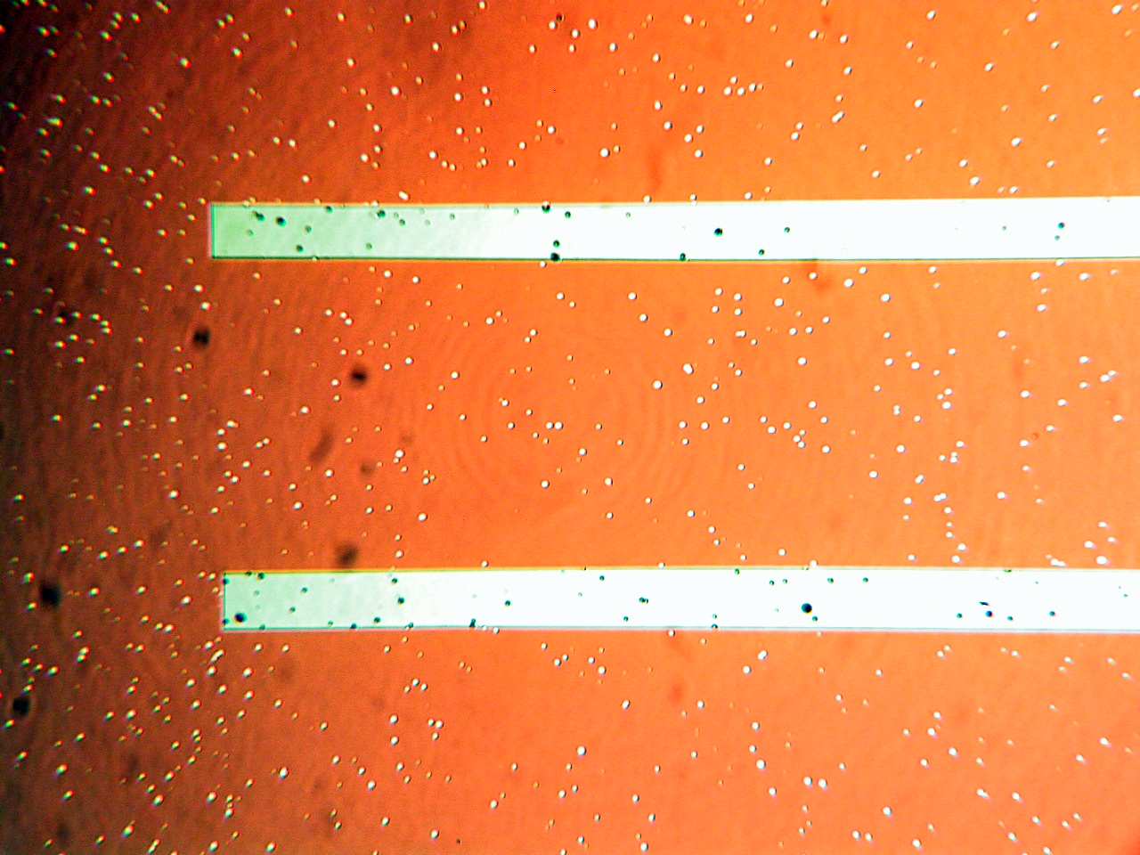 high density pinhole area
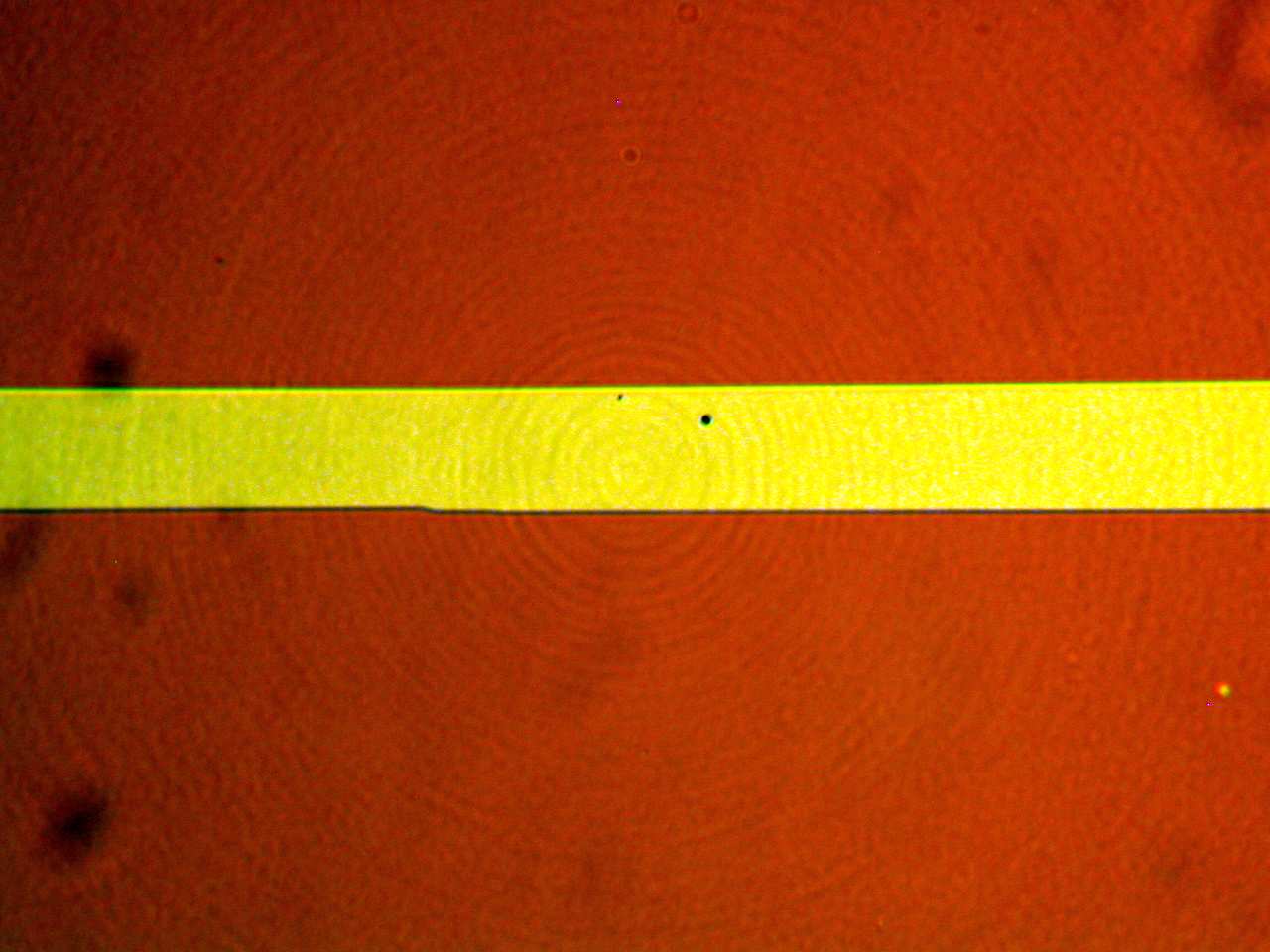 low density pinhole area
If there is any good news in this, it’s that the edges of the membrane seem to be free of debris under optical inspection. This complements Maryna’s burst tests. Now if we can just eliminate the pinholes we can finally get down to business. To strengthen the top sputtered oxide, we can anneal our film for a longer period of time in the RTP (essentially mimicking a furnace anneal). The room temperature deposition is also hurting us. Film density should increase after we get the heater back online.
Notes:
- TEM on campus was down Monday for plumbing work
- TEM @ URMC was unavailable due to 2-day training session
- I’ll try to get some EM done tomorrow afternoon when things are back online
- The sputter heater is nearly completed. We should have it online for this week’s depostion.