AFM
I took a sample from w304 over to the Krauss Lab and had them try to image it with AFM. Here are a few pictures (for some reason the color scales weren’t included in a couple of them, but they go from 0-dark to 5-light nm):
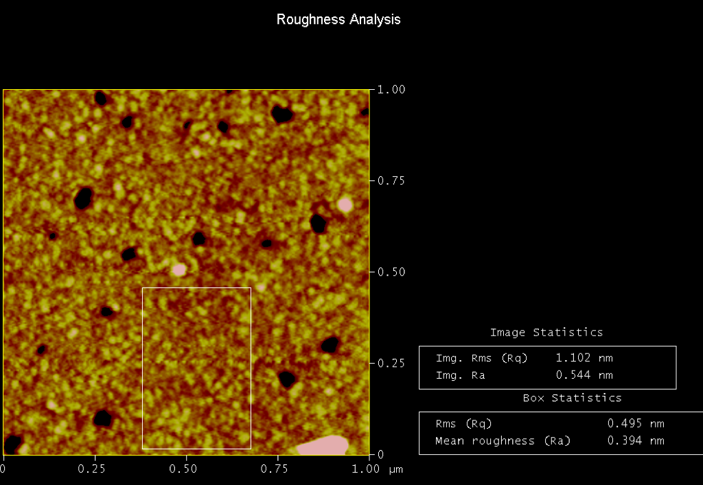

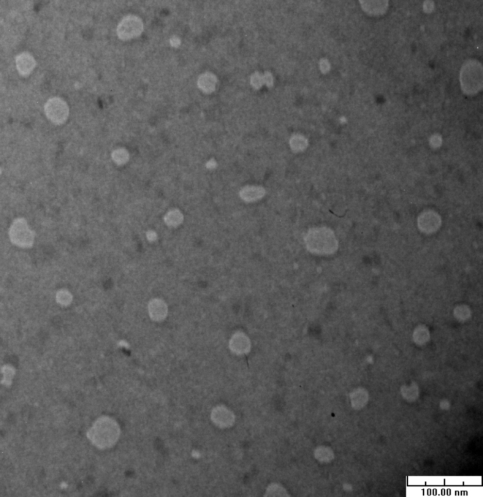
In both images you can surprisingly see the pores. The only go down to about 5nm from the surface plane. The tip is 10nm with a 20-30 degree cone, so the pores will appear smaller than they actually are. Here they appear to be about 25nm, and on the TEM they’re about 50 for this wafer (I specifically selected a sample with big pores). The first image also has some dust or particles on it.
The total RMS (including the pores) was about .7 nm for all the images except for the ones with particles. The RMS for areas without pores was about .5 nm. In the TEM images we see small divots that are probably not through pores. It appears that there are little bumps in the AFM image, and while they might be the nanocrystals, they could also be the pieces in between the divots.
We’re welcome to go back and use their system if we want to test more samples.
Here’s a TEM image fomr w403 for comparison:
Cool! I can make up some samples to look at the backside of the membrane to compare the shape/roughness.
This was done in a non-contact mode?
These are great images! Did Katie help you or do you have another contact in the Krauss Lab? This tends to be a very busy tool, so we should be careful not to overstay our welcome, especially since AFM can be so time-consuming.
This deserves a discussion, as there is a huge back-log of AFM work/studies that need to be done on our films. I assume that these images are the topography of the film on the wafer, off of the membrane? If so, Dave’s suggestion of imaging the backside of the same film would be quite useful.
Also, when I analyze the image, the larger pores seem to be about 50 nm, so I think everything makes sense. Please check. The effect of the tip is the sloping sidewall, but the true pore size seems to be resolved fairly well. The tip seems sharper than 10 nm to me.
The pore depth appears to have run out of range to me, so the depth cannot be trusted.
Joaquin Calcines helped me get the image. I told him we were going to try to figure out how to flip the film and he was willing to help look at it again. There is a backlog to this instrument; it took me about a week to get time on it.
I think they’re only set up to do tapping mode right now.
Chris, you’re right, some of those look close to 50nm. I’m surprised because the tip is apparently one of the cheapest you can get (it’s like 10 bucks per tip) and it’s supposed to be at best 10nm.
Chris, I forgot to add that yeah this is taken where the membrane is backed by the silicon support.