Nanoparticles on pnc-Si and pnc-Si pores via SEM
I’ve been thinking of demos/experiments to do with my upcoming class and one of them is SEM. I was thinking of handing out some unknown nanoparticle solutions and have them figure out the size and maybe material by SEM, AFM and/or DLS.
I’m approved to run the SEM now, so I hopped on today to image some of our polystyrene fluorescent nanoparticles as a test. I coated the sample first with 3nm of gold-palladium to reduce charging. This micrograph shows the edge of where I allowed the nanoparticle suspension to dry onto a SC048 chip.
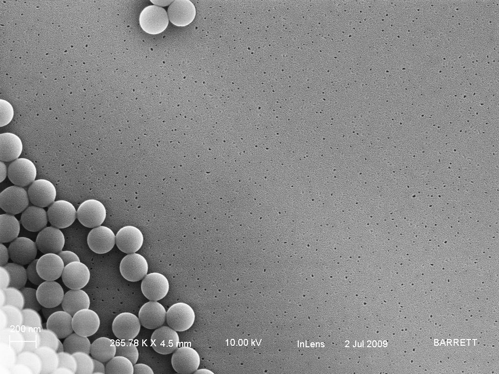
You can see the scanning specs on the bottom of the scan – 10kV accelerating voltage, InLens detector. The scale bar is kind of hidden above the bright nanoparticles at the left bottom – but it’s 200nm. This confirms the relative size of our particles. Since this is the very edge of where the NPs adsorbed, there is only a small monolayer and then the particles are dried on top of each other at the bottom left. Note that this is supported membrane.
Check out our nanopores – they look pretty good, I think, for SEM. I was able to resolve them much better with the inlens detector than the secondary electrons detector. Should we shoot to look at gold NPs blocking pores next?