Agglomeration verification
It seems that pores are only formed in the “sandwich structure” on certain process. So in order to verify this conclusion, I annealed two layers structure (20nm sio2+15nm si) to test the agglomeration theory. The other parameters in depositing and annealing are same to typical sandwich structure process (1000°C anneal, ramp rate 100c/s, w/o bias, no susceptor). The following SEM images proved the agglomeration even though with some strange but interesting phenomena.
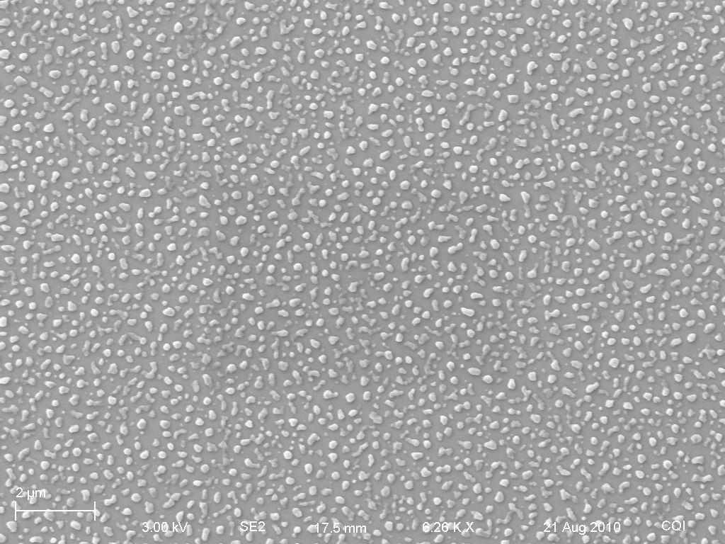
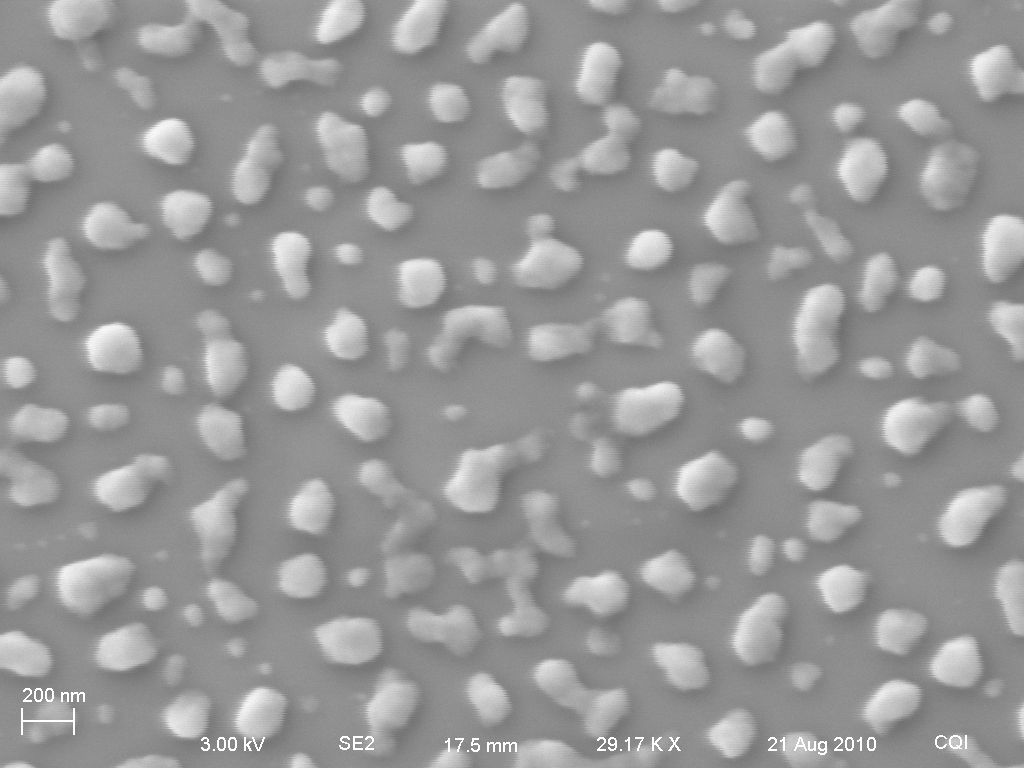
This image showed typical agglomeration happened to the top si layer. The average size of agglomerated island is around 200nm. However, besides agglomeration areas, I found some interesting areas with no agglomerated islands.

In this circular area, there is only one big island around 10um in the center without any islands surrounding.
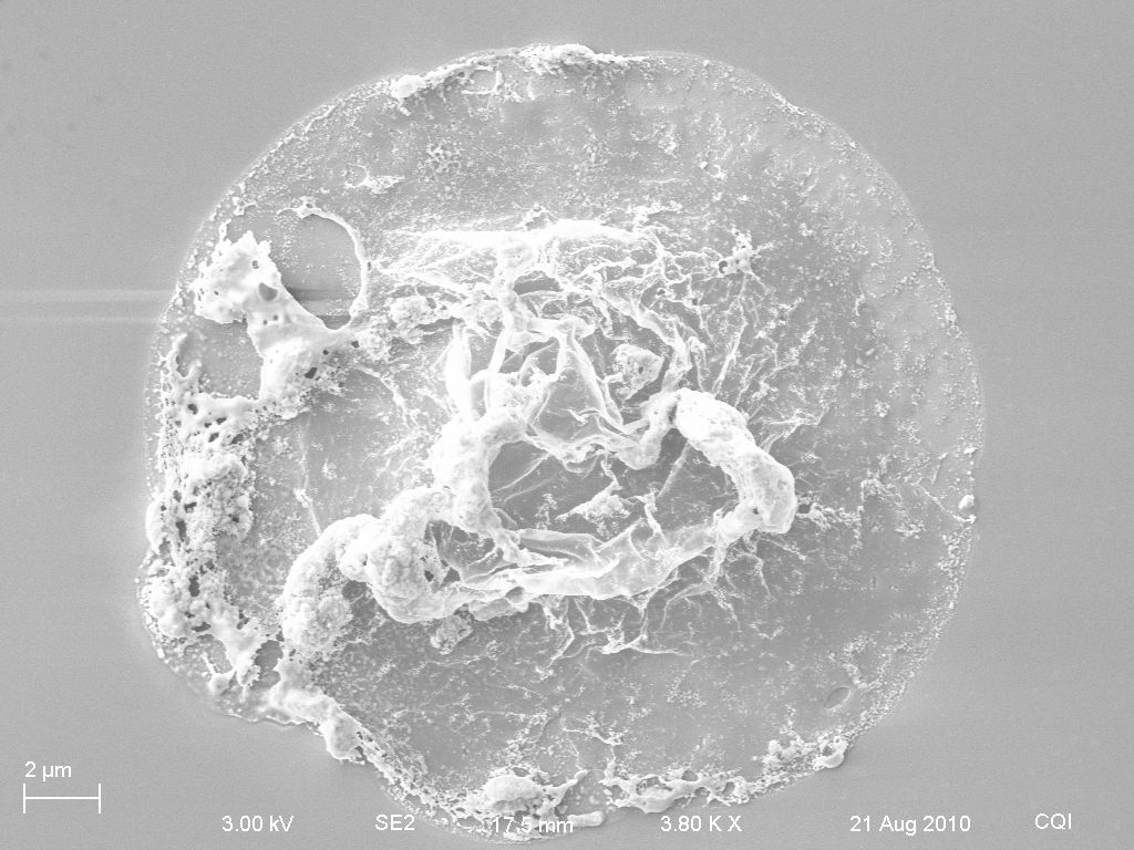
This is a zoom in view of the big center island. And there are a lot of these circular areas with a big center island in the whole wafer.

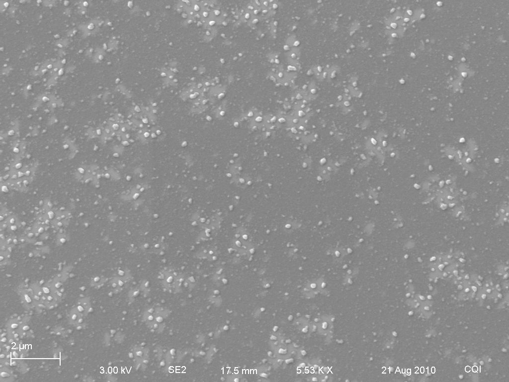
This is the edge of the circular area and you can see that the density of agglomerated islands is lower than that of the agglomeration area. I guess maybe those circular area are from some defects or contamination in the bare wafer.
Anyway, this experiment verified the theory of agglomeration in two layers structure, which proved the crucial effect of “sandwich structure” in pore formation on the other hand. Next step, I’m going to run a series of experiments with changing the thickness of top and bottom SiO2 layers separately to figure out how do they function in the pore formation.