pinhole-less membranes
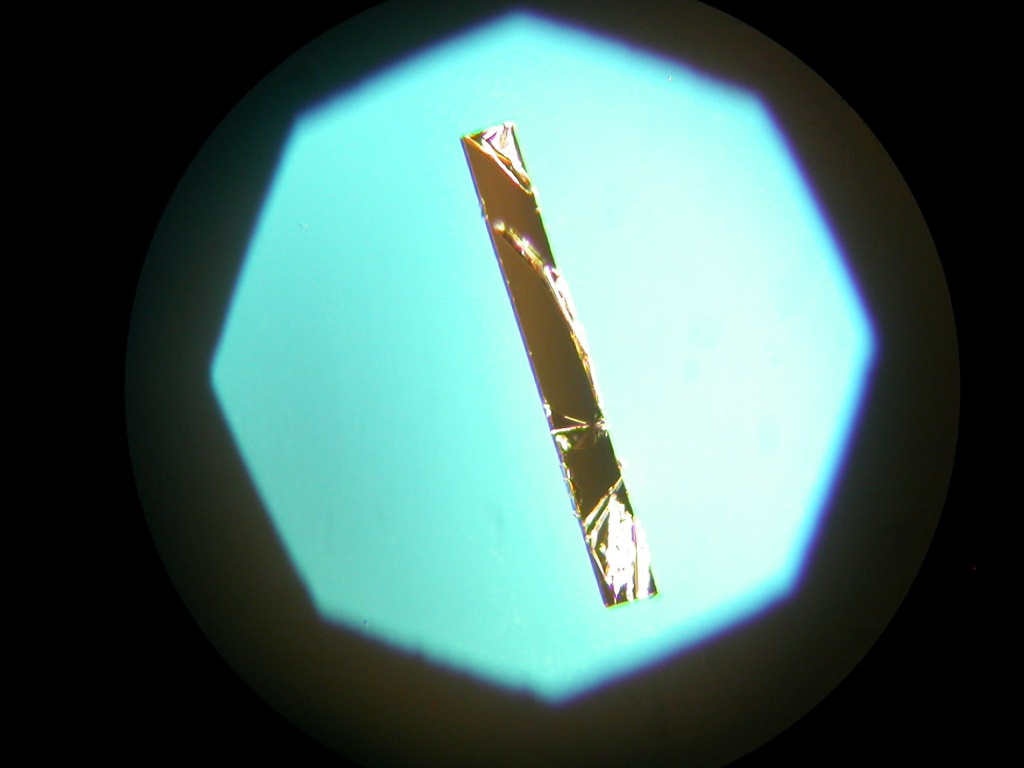
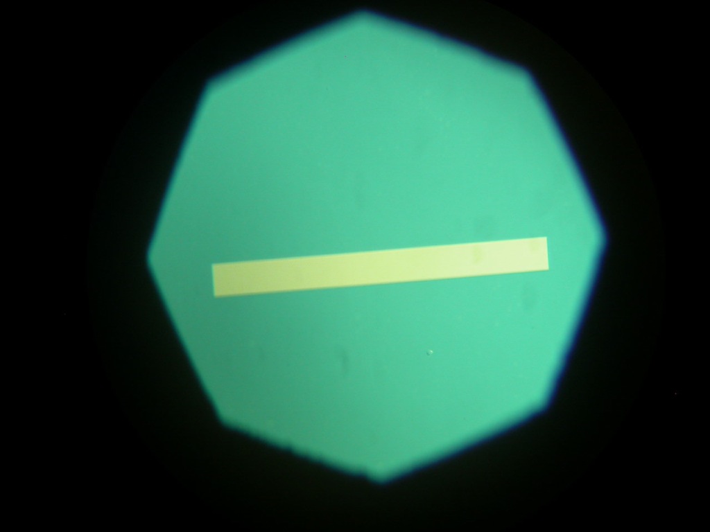
Inspired by JP, we decided to try to etch amorphous (unannealed) wafers this week to see if pinhole density changed. To my surprise, the amorphous membranes had no pinholes! Furthermore, I tried to anneal the membranes after the etch and they went flat indicating crystallization! Refer to the table below for the results.
Wafer 565: 40/15/40 stack; silicon etch THEN anneal
| position | condition | result |
| (1,1) | stripped oxide, annealed in open @ 950 C | broke in RTP |
| (-1,1) | oxide kept, annealed in open @ 950 C | flat after oxide strip |
| (-1,4) | stripped oxide, annealed in sus @ 950 C | broke in RTP |
| (1,4) | oxide kept, annealed in sus @ 950 C | flat after oxide strip |
| (-3,2) | stripped oxide, annealed in sus @ 800 C | flat after RTP |
| (3,2) | oxide kept, annealed in sus @ 800 C | broke during strip |
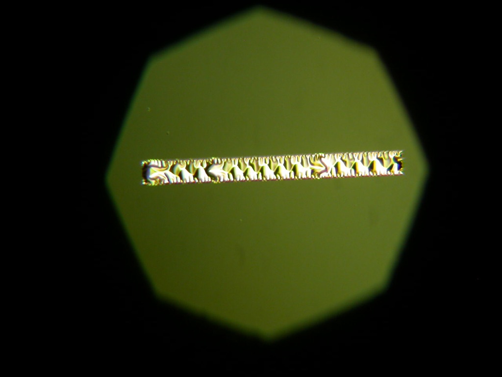
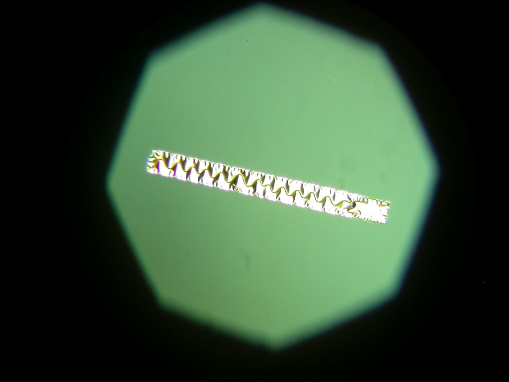
Wafer 574 was annealed at 950 C then etched (our standard process). Images below show that there are pinholes in these membranes. I should mention that the density of pinholes on this wafer is less compared with previous weeks…


Notes:
- Wafer 565 was not RCA cleaned, and wafer 574 was. Therefore, we can’t make a 1-1 comparison between the two. It is possible that the RCA clean may be causing the pinholes, but I think this is unlikely. We’ll test a wafer this weekend that will not have a RCA clean and run an etch first then anneal.
- The RTP and deposition chamber are not the cause of pinholes based on these results.
- We’re not sure if the etch/annealed wafers have open pores. We’ll confirm this next week on the TEM.
- This is bizarre; we’ll keep exploring…
you wrote … “annealed in sus”
what is “sus”?
“Sus” is susceptor. This is really the only reasonable way to anneal membranes, as we can only measure the temperature of the substrate in the RTP. Therefore the membrane temperature is unknown and would likely be nonuniform. The Susceptor creates an environment of highly uniform temperature for both the wafer and membrane.
This pinhole problem is starting to look like a wider surface contamination issue than a pure particle issue. Until we have all the tools that we need, working well and in controlled environments, these problems will continue. We will continually develop work-arounds, but these take time. We need to get the megasonics system. We need to get the silanization system with the plasma cleaning option. We need to get the new sputter system, RTP, and good inspection microscope into the hopeman cleanroom. All without delay. Unfortunately, for full humidity control, we’ll have to wait for Goergen to be built…
RCA clean causing pinholes?!
I have a ton of data, starting from last summer, showing that both RCA clean and “scrub” clean are effective in removing particulates.
I still believe the pinholes are due to dislocation centers and/or stacking faults due to thermal coefficient and lattice mismatch causing film cracking during a-Si film crystallization.
The reason I ran this experiment was to show that there are no pinholes in a-Si film (that has not been crystallized). Next, I will test wafers nearing and reaching the anneal temperatures.