Agglomeration(2)
Recently I did some further research on the agglomeration in SiO2+Si layers. On my first post about agglomeration,I found that after annealing at 1000ºC for 1 min without susceptor, 15nm thick Si layer agglomerated and the average diameter of agglomeration islands is around 200nm. This time, I deposited three different thickness of top Si layers which are 5nm, 10nm and 30nm. Then I annealed them at 900ºC, 1000ºC, and 1100ºC for 1min and 5min with susceptor, respectively. The followings are the SEM images of those samples. In order to find out how is the agglomeration affected, I arrange the images with three parameters, which are thickness, annealing temperature and annealing time.
1. Thickness
The following figures are samples with different thick Si layers annealed at same temperature for same time.
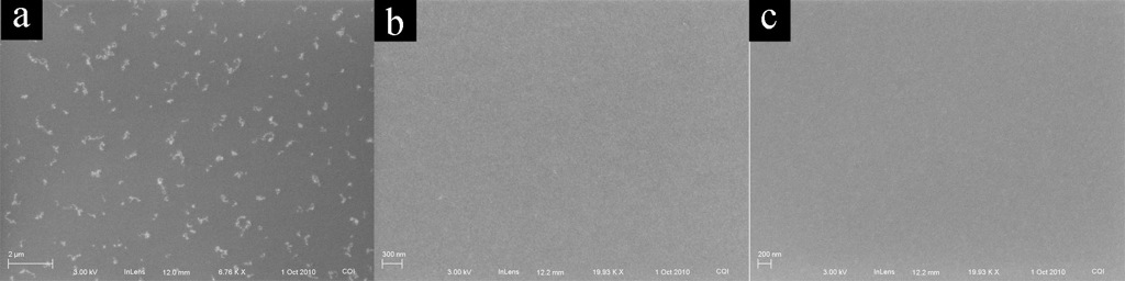
Fig.1 is three samples annealed at 1000ºC for 1 min, which (a) is 5nm thick, (b) is 10nm thick and (c) is 30nm thick, respectively. From this figure we can see a lot of narrow irregular agglomeration islands in 5nm thick sample. It is likely that the Si layer with 10nm thick starts to agglomerate as the surface looks roughly. However, no agglomeration shows up in 30nm thick sample. It indicates that annealing at 1000ºC for 1min is not enough for 30nm thick Si layer to agglomerate. As the film becomes thicker, higher temperature is needed for the film to agglomerate, which is quite reasonable.
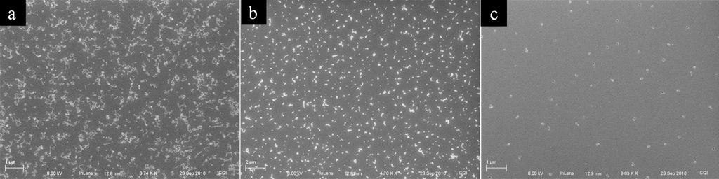
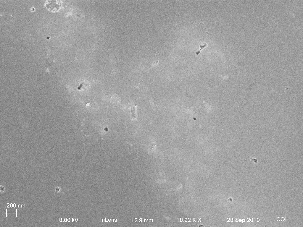
Fig.2 is three three samples annealed at 1100ºC for 1 min, which (a) is 5nm thick, (b) is 10nm thick and (c) is 30nm thick, respectively. Agglomeration islands are observed on all three images which means that three different thick Si layers all agglomerated after annealed at 1100ºC for 1 min. However, big differences between agglomeration islands not only in size but also in shape are also observed. It seems that for 5nm thick film, the agglomeration islands are more like thin narrow ridges. When the thickness of Si film grows up, those thin ridges turn to become big and round. Another thing which intrigues my notice is the shape of agglomeration islands in 30nm thick Si layer. They look more like pits than islands. Fig.3 is an enlarged image of those pits. Further investigation is needed to explain those strange shapes.
2. Annealing temperature
In this part, I make some comparisons among same thick samples which were annealed at different temperature for same time.
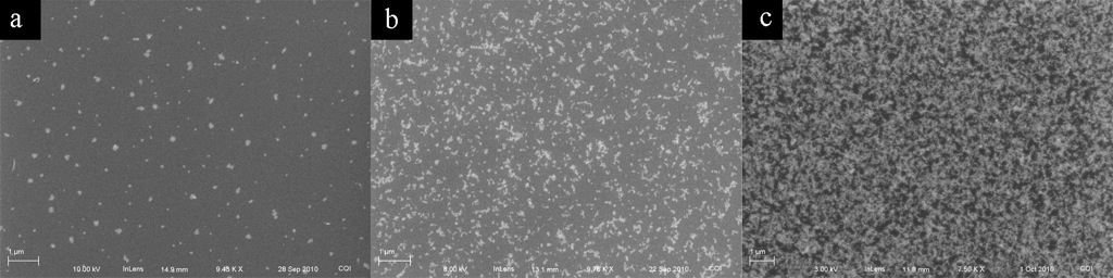
Fig.4 is 5nm thick samples annealed at three different temperatures for 5 min, which (a) is 900ºC, (b) is 1000ºC and (c) is 1100ºC. Compared these three images, it seems that with the increase of annealing temperature, more and more agglomeration islands are formed and they start to connect with each other. It could be explained by the following. Agglomeration islands are formed as a way to decrease the total free energy. Higher temperature annealing means higher energy is imposed into the system and more agglomeration islands thus are formed.
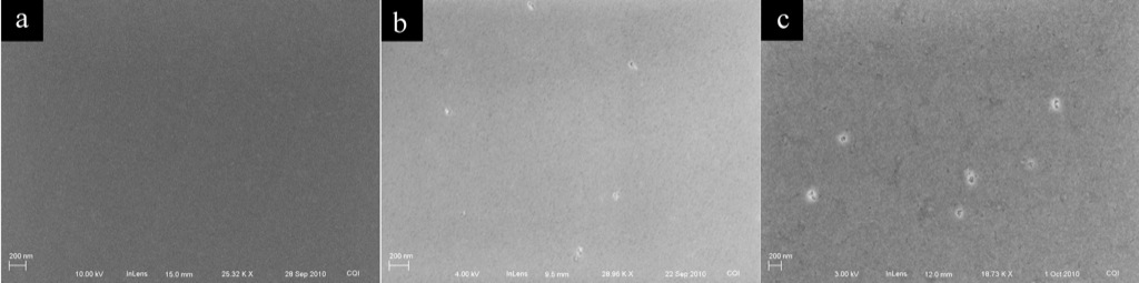
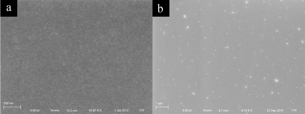
Fig.5 shows 30nm thick samples annealed at three different temperatures for 5 min, which (a) is 900ºC, (b) is 1000ºC and (c) is 1100ºC. At 900ºC, even annealed for 5min, the Si layer is still flat, which means annealing at 900ºC is not high enough to prompt the agglomeration. When temperature increases, the Si layer is not flat any more. Agglomeration takes place when annealed at 1000ºC and 1100ºC and the “agglomeration islands” formed at 1100ºC is larger than that at 1000ºC. More efforts are needed to figure out are those agglomeration islands holes or not.
3. Annealing time
Annealing time would also affect the agglomeration in Si layer. Fig.6 is 10nm thick samples annealed at 1000ºC for 1min(a) and 5min(b) respectively.
We can see that when the annealing time is only 1min, even the annealing temperature is as high as 1000ºC, no agglomeration islands are observed in 10nm thick Si layer, even though the surface looks quite roughly. However, when the annealing time increases to 5min, clear agglomeration islands are observed and average diameter is around 100nm. It indicates that annealing at 1000ºC for 1min with susceptor is not enough for 10nm thick Si layer to agglomerate.
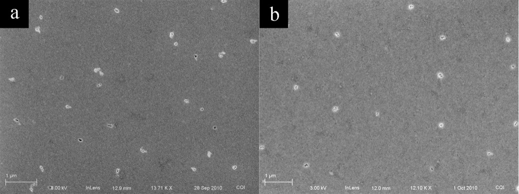
Fig.7 shows 30nm thick samples annealed at 1100ºC for 1min(a) and 5min(b) respectively. It seems that no big differences exit between the morphologies of 30nm thick Si layers which are annealed at 1100ºC for 1min and 5min, which indicates that at higher annealing temperature, annealing time would not affect the morphology of agglomeration very much.
Thickness, annealing temperature and annealing time are three main factors that would affect the agglomeration of Si film. It seems that the thickness of film is the key factor to determine the morphology of agglomeration islands. Annealing temperature and time are also important since they would also affect the shape of agglomeration islands.
Next step, I’m gonna try to get some detailed information about the agglomeration islands, especially in the 30nm series, and figure out how to extend the agglomeration to our three layers structure.
I’m not sure if it will be useful to continue working with the 30nm films, since they are not agglomerating. These are clearly holes, and the magnified image shows a “debris field” around these pits indicating that some destructive process is taking place. I don’t know if there is a reason to learn more about this effect, since it will likely consume a lot of time, and provide no insight into pore formation.
There appears to be some useful information in the 5nm and 10nm films. Are you going to do some type of analysis on the images to determine the size and density of the agglomeration? We need to get something quantitative out of these experiments, right? Then figure out how this info can be applied to our sandwich film structure?
Any plans to do some TEM on any of these samples? I think you could overcoat with SiO2 and then etch membranes. Since the SEM shows no crystal structure, it provide little info regarding the film morphology.
It seems that the shape of agglomeration islands are quite different for 5nm sample and 10nm sample. I’m thinking ask Brian to help me do some real AFM images to see how large are the agglomeration islands and calculate the densities.
As respect to TEM test, the samples I made are those singe side polish without patterned wafers. Is there possible way that I can etch them so that TEM can be used? Thanks.
IF you cannot get high enough resolution with SEM, AFM may be better. It would probably give you better topographic information, depending on how high the islands are. If they are over ~100nm tall, you will need to be careful interpreting the data, since the tip shape will have a strong influence.
For TEM, you would need wafers with a backside pattern. You would run the experiment in a similar fashion, but after agglomeration, you would need to sputter an additional 20-50nm of oxide to protect your islands from the EDP during the etch. You could then try to image these samples with the oxide on them. IF you find that you cannot image well with this much oxide, you can try to strip some of it away, but you’d need to be careful to not remove too much, or the membranes would fall apart (assuming no Si between the islands).