In-situ TEM observation of pores movement from Harvard
A few weeks ago, professor Mike Aziz in Harvard University helped to annealed two samples and in-situ imaged the early stage of pore formation using their Jeol2010-hot-stage-TEM. The oxide seemed intact during the process. The sample was unannealed 20(bottom)/15(a-si)/10(top) three stack with removing the substrate.
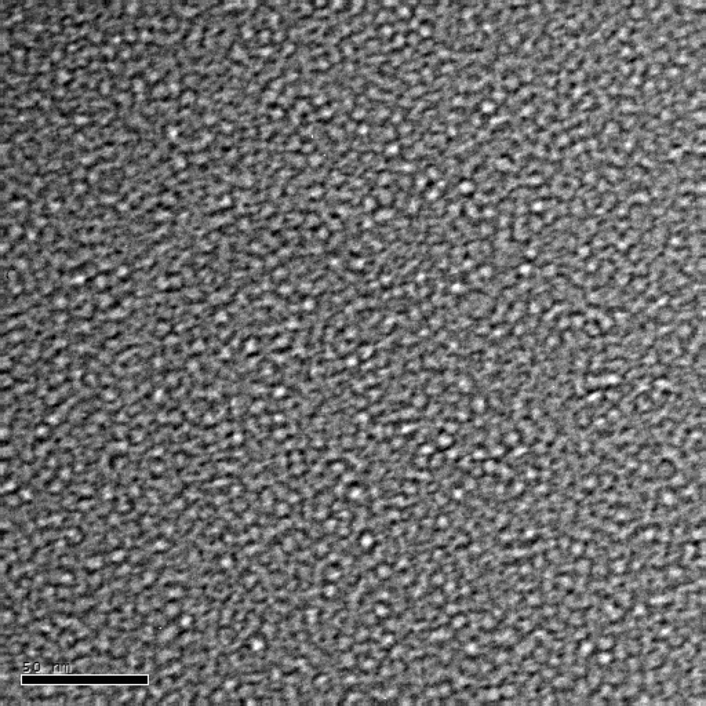
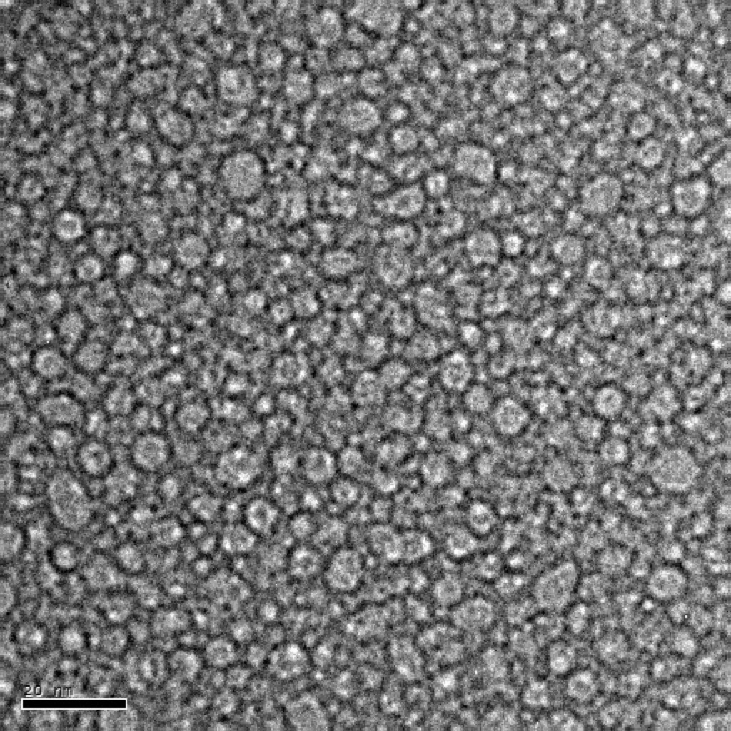
The first sample was heating to 693C. They took one image every three seconds. For first 5 minutes at 693C, they observed 5-10 nm morphological features but diffraction pattern was still amorphous.
After maybe 5 minutes the first diffraction spots appeared and 2 minutes later a nanopore poped open and it was not equiaxed. Then they hold the temperature for10 minute, watching pores formed and ended up at 694.42C. I made a movie by connecting the images together.The following movie showed pores moved around and some coalesced.
Some points I want to emphasis in this movie:
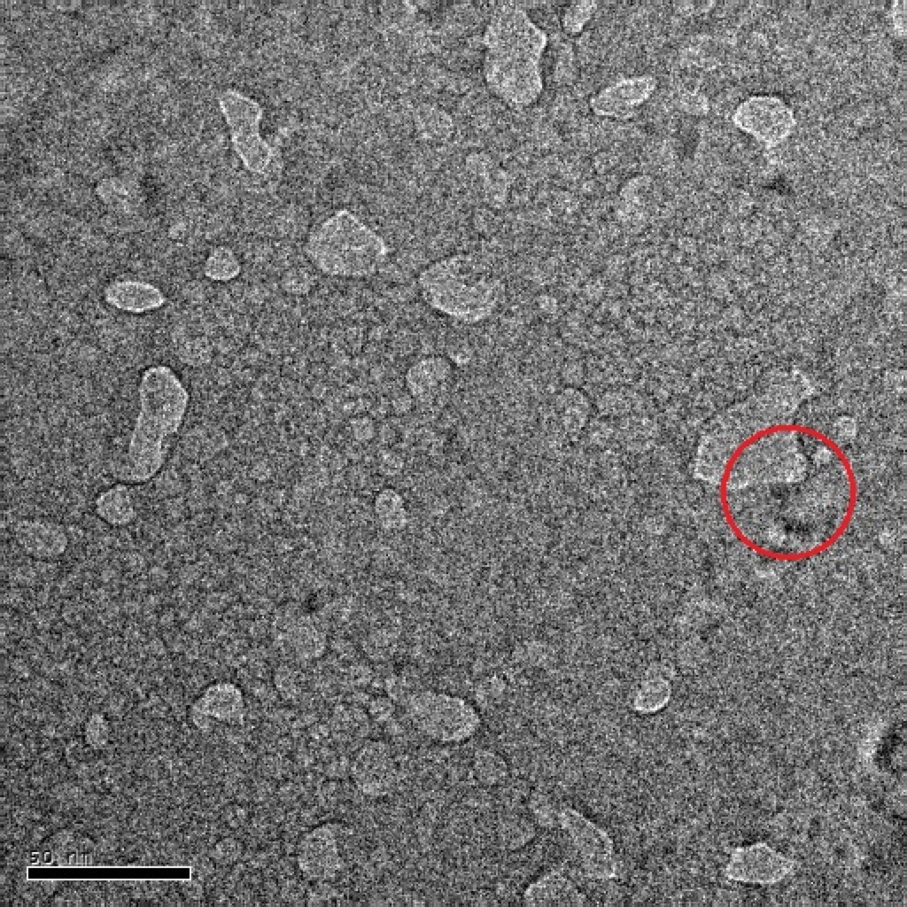
1. Pores were moving around in different directions and it seemed to happen in amorphous area, e.g. the area in the middle center.
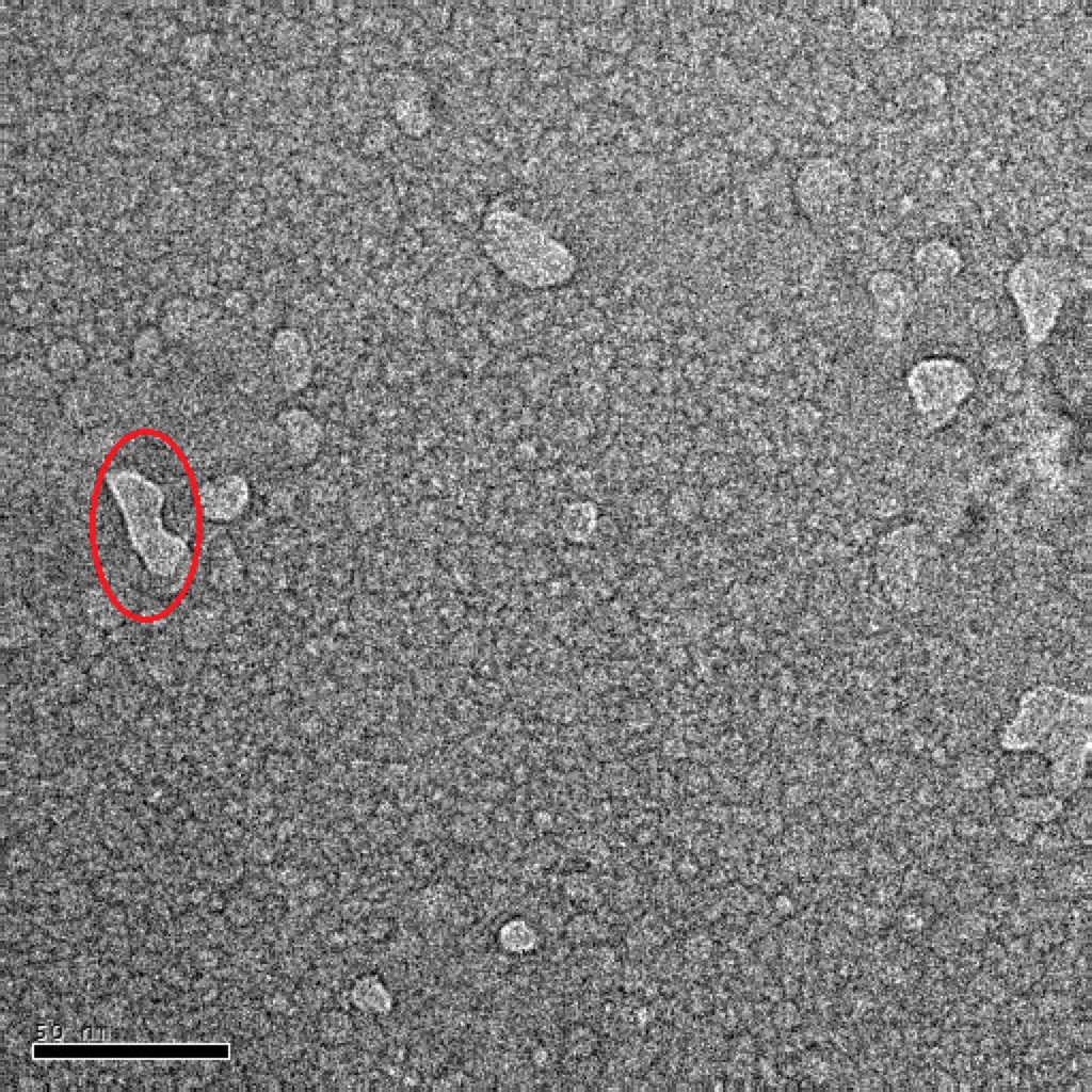
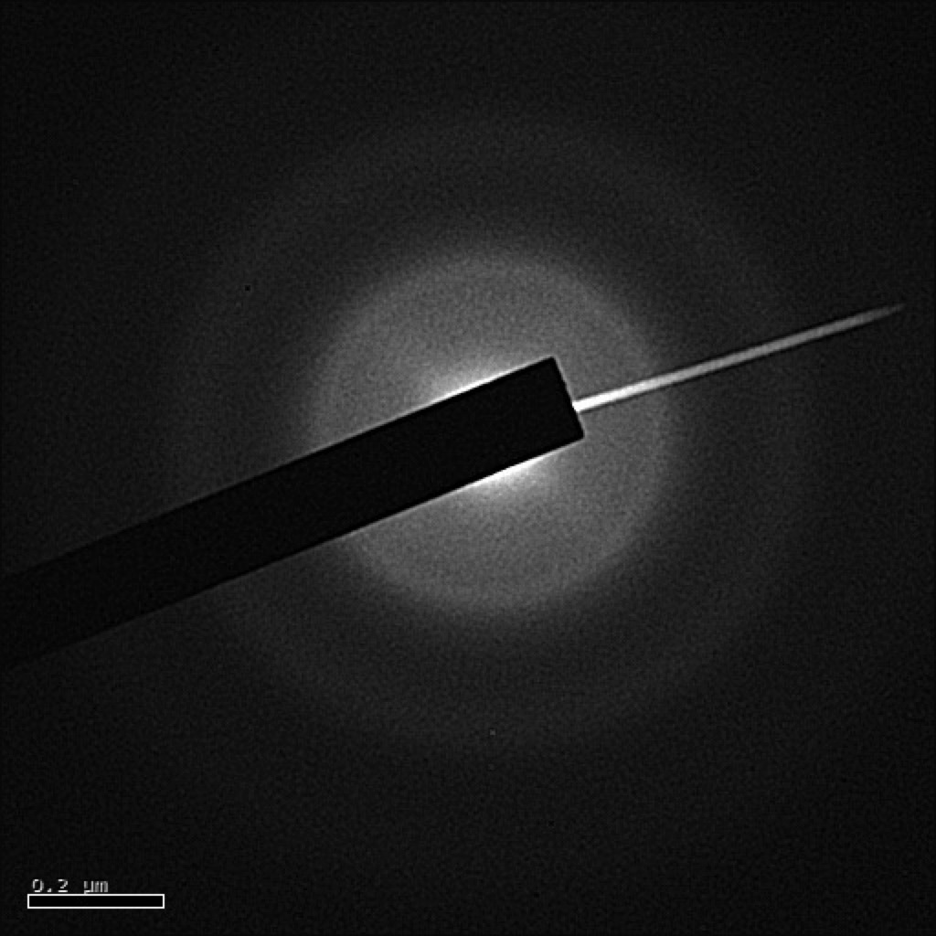
2. Some pores didn’t move at all. See the circled pore in the image below.

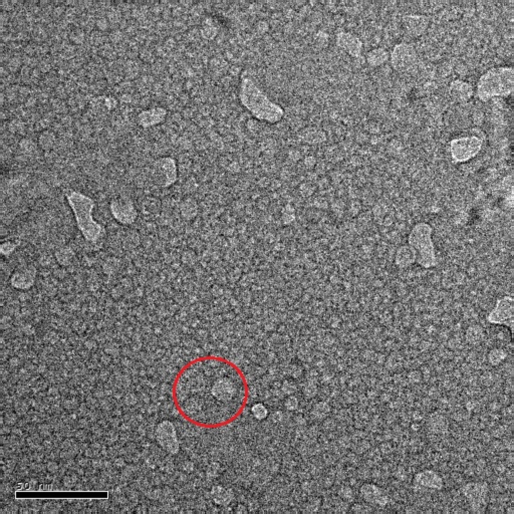
3. New pores showed up and they tended to coalesce to form big pores during moving.
4. Pores were immobilized once they touched Si crystals (black area). I think this might be the reason for the necklace pattern of pores Dave observed.

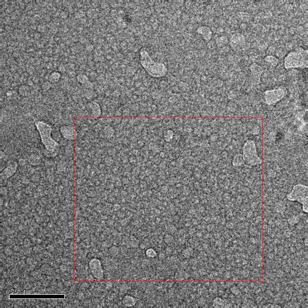
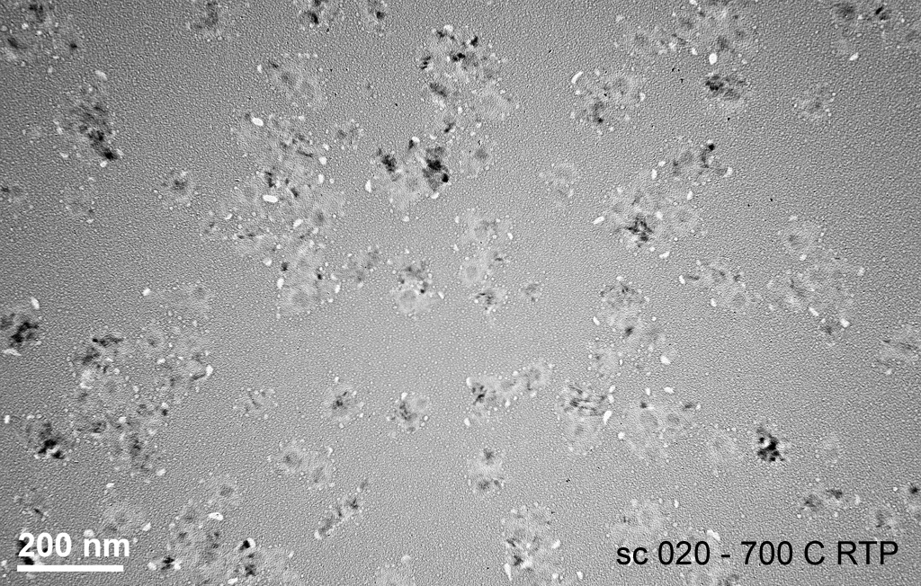
After cooling down to room temperature, pores were enormous and irregular in shape.

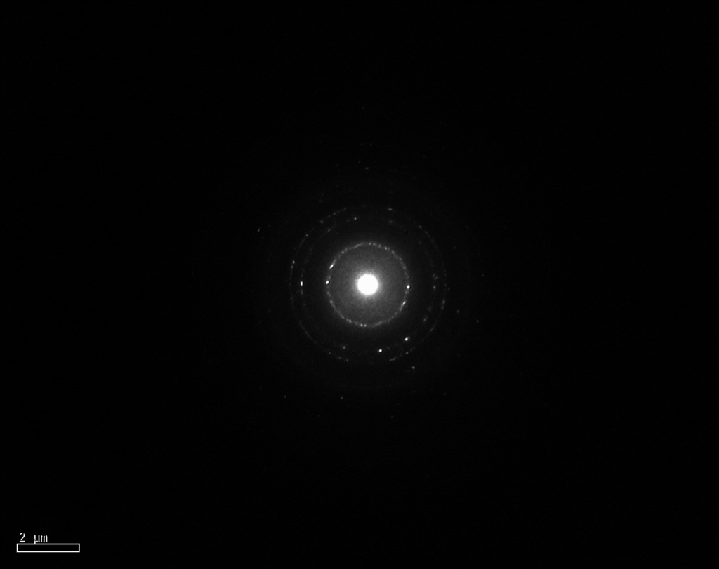
The diffraction pattern showed crystalline rings and confirmed the nanocrystalline structure in first sample.
For the first sample, it seemed that pores were more likely formed in amorphous area and they were moving around to coalesce with each other to form bigger pores. The pores seemed to be immobilized once they touched the Si crystal.
For the second sample, they planed to go rapidly to 690 C and hold to take images. This time, they took one image every two seconds. They hold the temperature at 690C for approximately 3 minutes then cut the power off to quench the sample and they found huge jump in images due to too-fast drift. The last image during the quenching was taken at about 300 C. I combined all the images to make the second movie. A 1 second pause in the second movie represented the start of the quench.
When the temperature dropped back to room temperature, they took another image.
The diffraction patter of this image showed that it was still fully amorphous.
From the second movie, we can clearly see the change of morphology. It looked like that the Si atoms in the amorphous layer were moving around and I believe this is the initial stage of crysatllization. If we carefully compare the TEM image of second sample at room temperature with the first movie (first sample), it seemed that the morphology in the TEM image was somehow similar to the first movie when pores were starting to form. It could also be seen by comparing the holding time. Si crystals and pores started to show up after 5 minutes annealing at 693C in sample 1 where sample 2 was only hold at 690C for 3 minutes.
Anyway, this in-situ TEM is very helpful to discover the pore formation mechanism. Pores and Si crystals are starting to form around 700C. We are still not sure which one comes first. However, pores seem to form in amorphous area and they are moving around to coalesce and form bigger pores during forming process. Si crystals seems to immobilize pores when they are adjacent to each other.