The onset of pore formation in NSN and OSO stacks
A few weeks ago, I did some RTP annealing of NSN and OSO stacks. The purpose of this annealing experiment was hoping to capture the onset of pore formation and see whether there is any different behavior between NSN and OSO stacks. The annealing temperature was set to 700C. The ramp rate was 50C/s all the time. The annealing time varied from 1s to 5s, 10s, 30s and up to 60s.
The first TEM image series are from NSN stacks after RTP annealing. The TEM images clearly capture the onset of pore formation in NSN stacks. After 1s annealing at 700C, a few of silicon nanocrystals surrounded by pores are formed in the amorphous silicon matrix. These ”pearl necklace” silicon nanocrystals disperse around and they barely touch each other. When the annealing time increases to 5 seconds, lots of ”pearl necklace” silicon nanocrystals are formed in silicon layer. They start to tough with the adjacent ones. Both the density of silicon nanocrystals and nanopores increase with longer annealing time. It indicates that the nucleation speed is quite fast since the interval is only 4 seconds between those two scenarios. The crystal size doesn’t change much, which indicates that the crystal growth speed is not very fast. This means the nucleation dominates the current crystallization process.
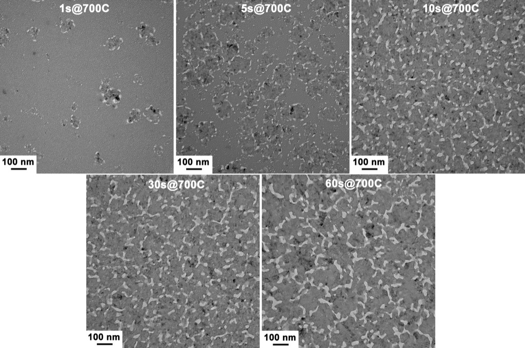
After annealing at 700C for 10s, the silicon nanocrystals and the nanopores are all over in the silicon layer. ”Pearl necklace” feature can no longer be seen, which is probably due to the coalescence of silicon nanocrystals as well as the nanopores. The coalescence of nanopores is quite obvious in the TEM image, which is the reason for the irregular shapes of nanopores. Besides the irregular pores, there are also lots of small round pores. The average size of those irregular pores is bigger than the previous two scenarios. The majority of phase of the silicon layer is nanocrystalline and there is very few amorphous phase left. This means that the nucleation stage is already done during the crystallization process in this scenario. This also tells us that it probably takes around or less than 10 seconds to crystallize the silicon film in NSN stack at 700C. Nanopores coalesce with adjacent ones during this period. When the annealing time is even longer, for example, 30 seconds, even 60 seconds, the morphologies of these two scenarios are kind of similar as that of 10 seconds annealing. Lots of irregular pores are formed in these two annealing scenarios. However, by careful comparing the 10s, 30s and 60s annealing, it seems that small round pores gradually disappear with longer annealing time. As a result, the density and size of the irregular pores, which is believed the final shapes of coalesced pores, become bigger with annealing time. Another interesting phenomenon is that the size of silicon nanocrystals becomes bigger with the annealing time, which makes sense.
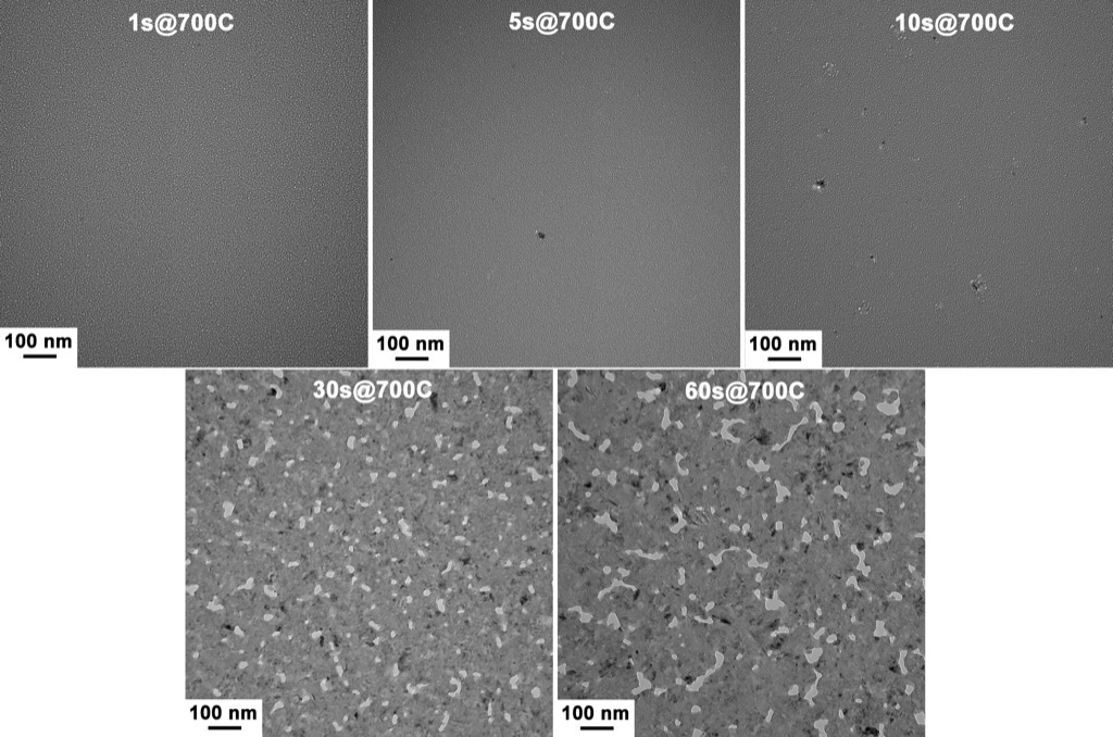
The second TEM image series are from OSO stacks. With same heat treatment, OSO stacks show a different result. No crystals can be seen in silicon layer after 1s annealing at 700C. The silicon is still complete amorphous. When the annealing time increases to 5 seconds, only a few of silicon nanocrystals are formed in the silicon layer. No clear pores can be seen from the TEM image. Even after 10s annealing, very sparse silicon nanocrystals can be seen in the silicon layer. The majority of the silicon film is still amorphous. After annealing for 30 seconds, silicon film is mostly crystallized and irregular nanopores are all over the silicon film. The size of nanopores grows bigger when annealed the OSO stack at 700C for 60 seconds and this trend is in accord with that from the NSN stacks.
After comparing the annealing results of NSN and OSO stacks, a few differences can be seen. The first one is that the crystallization starts earlier in NSN stacks than in OSO stacks. In other words, the crystallization of silicon layer in enhanced when sandwiched between nitride layers than oxide layers since they are in the same thickness. Another difference is that the pore size and pore density from NSN stacks are obviously bigger than those from OSO stacks, which is in accord with the previous experiments. This maybe due to the enhancement of silicon crystallization. Since the pore formation is directly related to the silicon crystallization, it is more likely the silicon crystallization enhancement also helps to enhance the pore formation.
Both the results from the furnace annealing and RTP annealing show that pores with bigger size and higher density are formed in NSN stacks compared with OSO stacks. The reason behind this difference is probably due to that the crystallization of silicon film is enhanced when it is sandwiched between two nitride layers than sandwiched between two oxide layers. The next step is to further investigate the what is the reason for this enhancement.