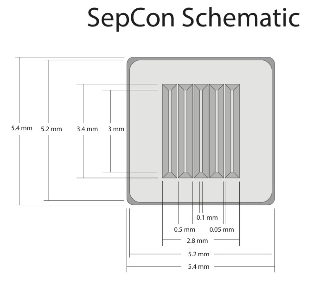
Using Alumina Deposition to Modulate Pore Size
The Cambridge Microsystems Savannah 200 atomic layer deposition (ALD) system uses a two-step chemical process that alternates pulses of water vapor and trimethylaluminum (TMA) to build a layer of Al2O3 on a silicon substate. Because of the two-step nature of the process, the film is forced to grow by successive monolayers, each with a thickness of 1.1 Angstroms (although this thickness is mildly temperature dependent).
NRG has been using Alumina to precisely control pore sizes since 2010. David Fang used a series of increasingly thick depositions to show that sieving coefficients for gold nanoparticles and hydraulic permiabilities match theoretical predictions based on the TEM images of ALD-ed chips. Tom found that thin layers (2.5 nm) of Alumina increased burst pressures of pnc-Si, while 5 nm decreased burst pressures. Dave found that Alumina doesn’t substantially change the contact angle of pnc-Si.
Because of the difficulty (and expense) associated with getting different pore size distributions, we’ve decided to switch over from ordering different pore distributions from Simpore, and instead purchase just one size of ~30nm average pore size and use ALD to shrink the pores as needed.
In addition to being cheaper and more flexible, this approach also will aid me in the construction of a theoretical model for the diffusion and convection of species through pores not much larger than the average size of the particle. It’s easy to imagine a set of experiments where the sieving coefficient of gold (and eventually, BSA) is measured through a variety of applied pressures, gold sizes, and average pore diameter. In fact, when I first joined the lab I did some very similar work.
Alex Mann was nice enough to instruct me in the vagaries of the ALD, and under his supervision my first depositions were gorgeous:
Non-ALD chip:
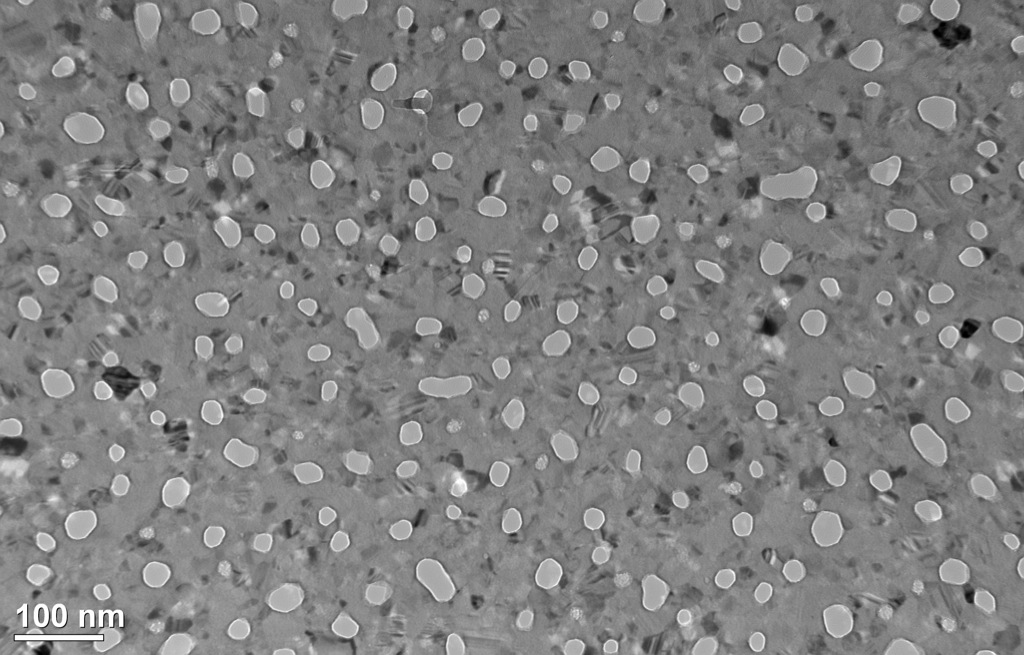

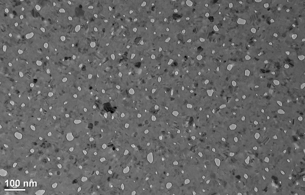
Avg. pore diameter 24.1 nm porosity 11.1%. For reference, Josh Winans found 26 nm avg. pore size and 12% porosity. It’s PFI wafer 852, which is 20 nm thick.
Using Jim’s Matlab hydraulic permeability code the theoretical permeability is 2990 uL/min-PSI-cm^2. Experimental permeability: 2337.8 (based on 5PSI, 0.015cm^2 active area, and 263uL of filtrate (determined by weighing) after 90s)
***
Chip after 25 ALD cycles (2.75 nm Al2O3 deposited, average pore diameter should be 5.5 nm smaller, membrane should be 5.5 nm thicker, assuming that the alumina coats both the front and back):
Actual average pore diameter 15.5 (expected 18.6); porosity 8.08%
Theoretical permeability: 1047 uL/min-PSI-cm^2 (4.8 PSI, 25.5 nm thick). Experimental permeability unavailable.
***
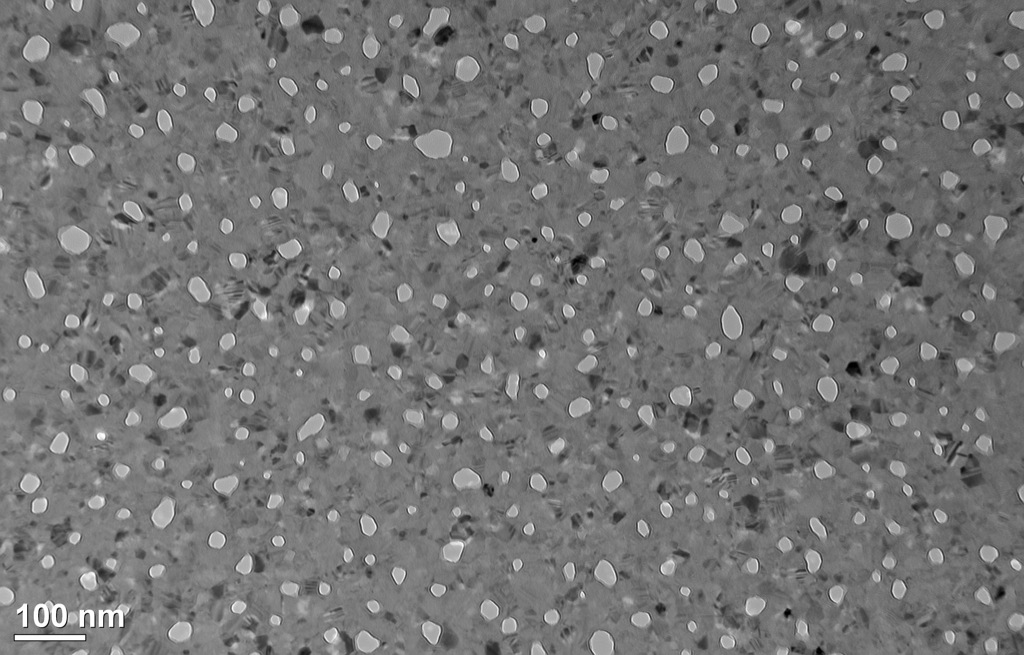
Chip after 50 ALD cycles (5.5 nm Al2O3 deposited, average pore diameter should be 11 nm smaller):
Actual average pore diameter 11.6 nm (expected 13.1); porosity 4.79%
Theoretical permeability: 391.85 uL/min-PSI-cm^2 (4.8 PSI, 31 nm thick). Experimental permeability: 299.38 (4.8PSI, 4min30s, 97uL)
Chip after 75 ALD cycles (8.25 nm Al2O3 deposited, average pore diameter should be 16.5 nm smaller):
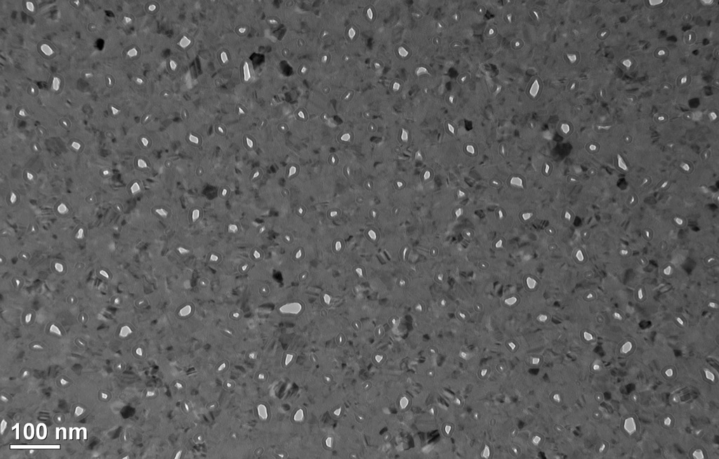

Actual average pore diameter 7.7 nm (expected 7.6); porosity 1.81%
Theoretical permeability: 75.12 uL/min-PSI-cm^2 (4.8 PSI, 36.5 nm thick). Experimental permeability: 67.59 (4.8PSI, 15min, 73uL)
The problems began once Alex left. Although we modified the standard ALD recipe slightly so that chips wouldn’t be blown around by the gas flow, my chips were troubled by the turbulent air.
First, this is how I braced the chips when Alex was there:
Later, I came in with a fatal optimism and attempted to do five of each size successively. I braced them like so:

Alas, disaster:

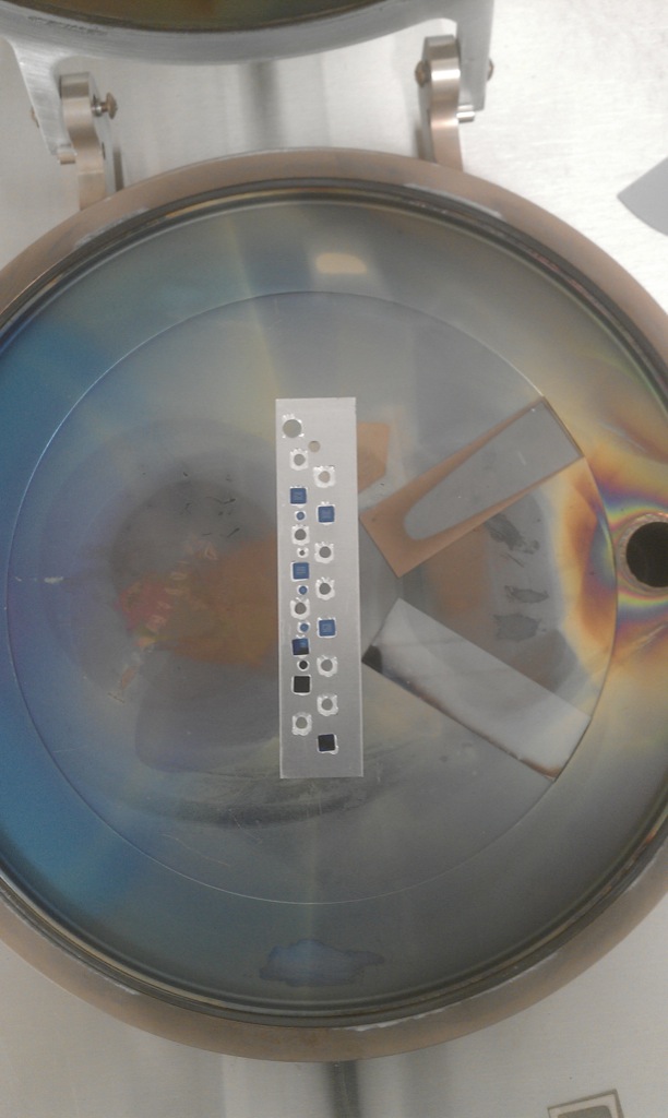
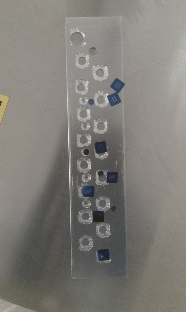
So I spent a day ginning up a little holder for my chips. I had SMC metal on 95 Mt. Read Blvd (off of Buffalo road) cut me a 1″x5″ 40 gauge piece of aluminum, that I then shaped using our drill press and the metal shaving dremel bit (apparently the dremel itself is missing the proper chuck required to hold that bit). The end result was this:
Alas, again, bad news:
After much cursing and careful examination of the ALD, I determined that it wasn’t the pulses of gas that were upsetting the chips, but either the initial pump down (which manifests itself as an audible ‘whump’) or the final venting to atmosphere. Even full glass coverslips would be noticeably disturbed if left unbraced in the center of the plate after a pump down and vent. The ALD doesn’t allow the speed of the vacuum to be adjusted, although it’s possible we can adjust the flow of nitrogen with regard to the venting process.
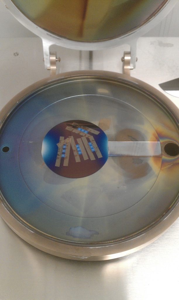
As a temporary measure until I can figure out something better I switched to using Kapton tape:
Josh pointed out that Kapton might outgas things that could disrupt the film, and so I avoid it for as long as possible. But it turns out that ALD is remarkably robust, and these jokers were actually able to use Heineken beer as the oxygen source (instead of water vapor) and get high quality Al2O3 films. Alex told me he has seen Kapton do weird things to the flow of gas, especially with platinum films. Also, it’s quite difficult to work with when dealing with a large number of free samples.
Of the twelve chips shown in the Kapton taped rig, most of them passed visual inspection and seemed to survive an unusually careful assembly, but broke once filled with water and pressurized to 5-6PSI. I was able to collect data on one of the 50 cycle and one of the 75 cycle chips, and I also collected data on an uncoated chip.
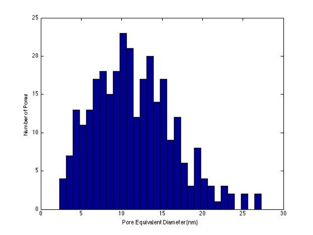
I ginned up a standard curve for 10 nm gold nanoparticles and collected approximately 200uL of filtrate from each of the three chips – 0 cycle (24 nm), 50 cycle (11.6 nm), and 75 cycle (7.7 nm). Gold concentrations did decrease as pore size decreased.
Below is a summary of all of my data:
| # ALD cycles | expected pore size | actual pore size | porosity (%) | theoretical permeability | experimental permiability | permiability with gold | sieving coefficient of gold |
| 0 | X | 24.1 | 11.1 | 2990 | 2337 | 1325 | 1 |
| 25 | 18.6 | 15.5 | 8.08 | 1225 | X | X | X |
| 50 | 13.1 | 11.6 | 4.79 | 533 | 299 | 147 | 0.135 |
| 75 | 7.6 | 7.7 | 1.81 | 120 | 68 | 33 | 0.035 |
Nice progress!
I don’t follow why you could not stick with the methods that were working with Alex for holding chips.
Also, are you increasing the membrane thickness in the model when calculating theoretical permeability?
Can this be done on a whole wafer? Or will it forever be confined to a handful of chips?
There was no method that I used when working with Alex – I think we just got lucky that the chips didn’t blow around. I did make sure to input the correct thickness for the permeability calculations (20 nm). The ALD is designed to work with wafers, so doing whole, half, or quarter wafers should be no problem at all.
I’m sorry if I’m being dense here. There isn’t a single membrane thickness for the theory – it depends on the ALD case we are talking about. Deposition closes pores and thickens membranes.
That’s an excellent point. I updated the permeability numbers to reflect the increasing thickness of the membrane as more alumina is deposited, and the theoretical permeability is now much closer to the experimental permeability. For instance, after 50 cycles, the calculated permeability without including the increased thickness was 533 uL/min-PSI-cm^2. Including the thickness of the ALD (we increase the thickness of the membrane from 20 nm to 31 nm, since 5.5 nm has been deposited on both sides) drops this number to 391 uL/min-PSI-cm^2, which is substantially closer to the experimental value of 299 uL/min-PSI-cm^2.