Nanoporous SiN Membrane Coated with Gold Nanoparticles
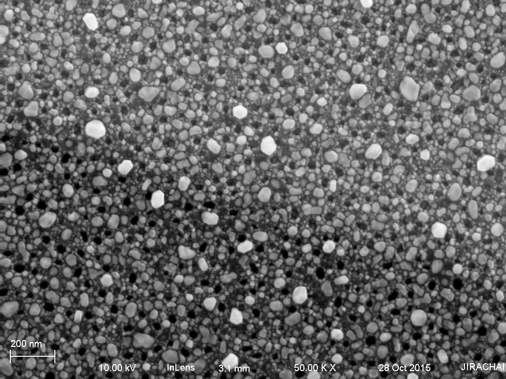
It was expected that heating up the substrate during Au sputtering would help increase mobility of Au into nanopores so that the uniform coating on pore wall could be achieved. The result was quite unexpected; Au did not coat uniformly on pore wall nor the surface of membrane. Instead, Au clumped into nuggets of various nanometer-scale sizes all over the membrane and into the pores, except on the back side. Below are SEM images of a nanoporous SiN membrane coated with Au nanoparticles.
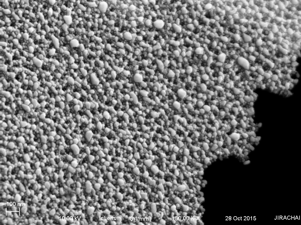
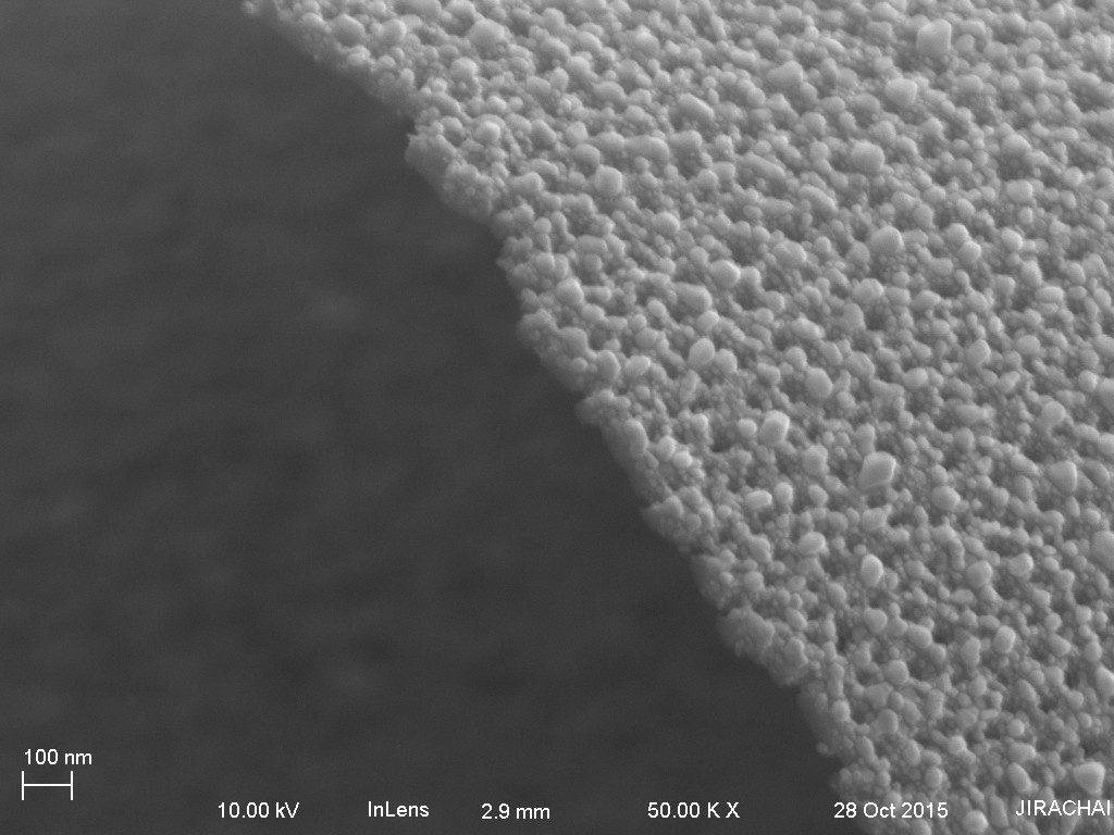
Something like pebbles on the membrane surface are gold. The biggest one is almost 100 nm. A view from another angle gives a peculiar feel of texture on the surface of membrane.
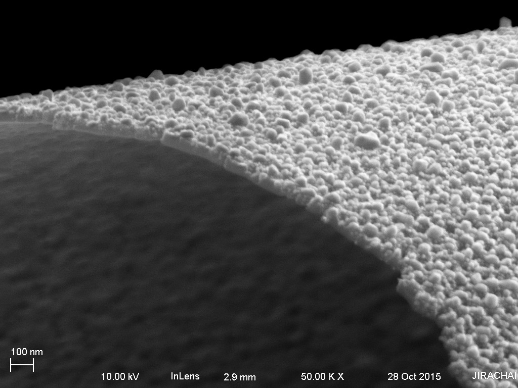
The cross-sectional view of the broken membrane reveals that some small Au nanoparticles can be found inside the pores as well. Were they formed inside the pores or did they fall into the pores?
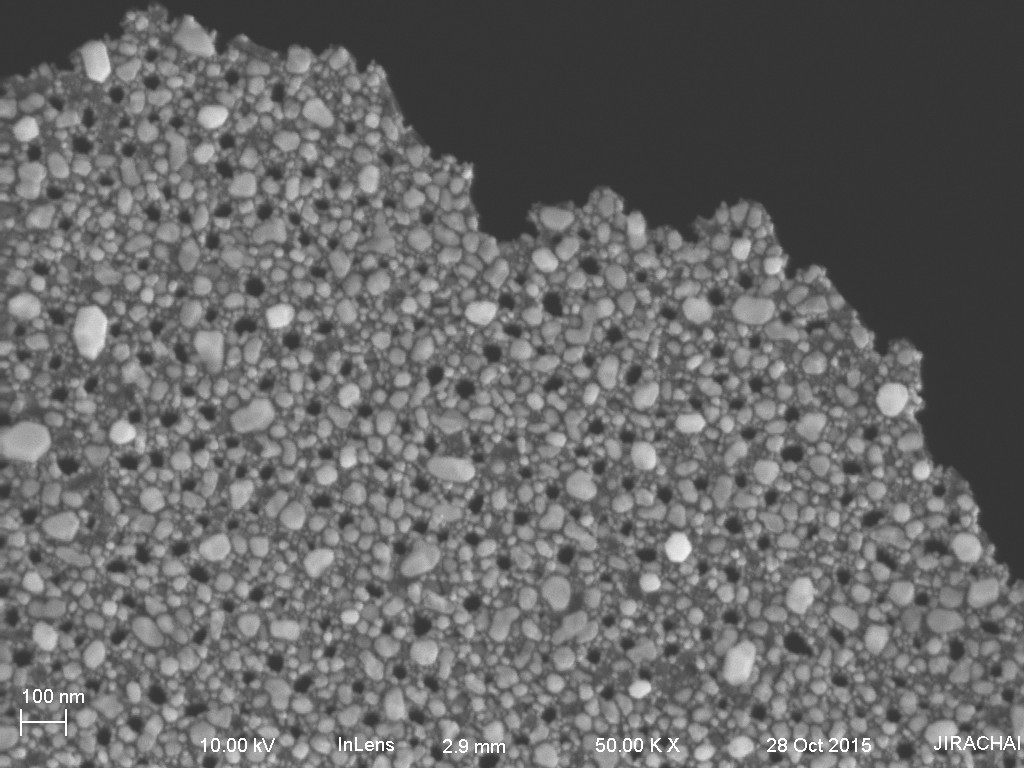
It seems that they do not occlude all the pores of the freestanding membrane, but they fill the pores of the membrane on Si substrate.
Like normal Au sputtering, Au nanoparticles are not found on the back side of the membrane. Interestingly, a view from the back side reveals that Au actually coat on the pore wall. It is more evident along the edge of the broken membrane.
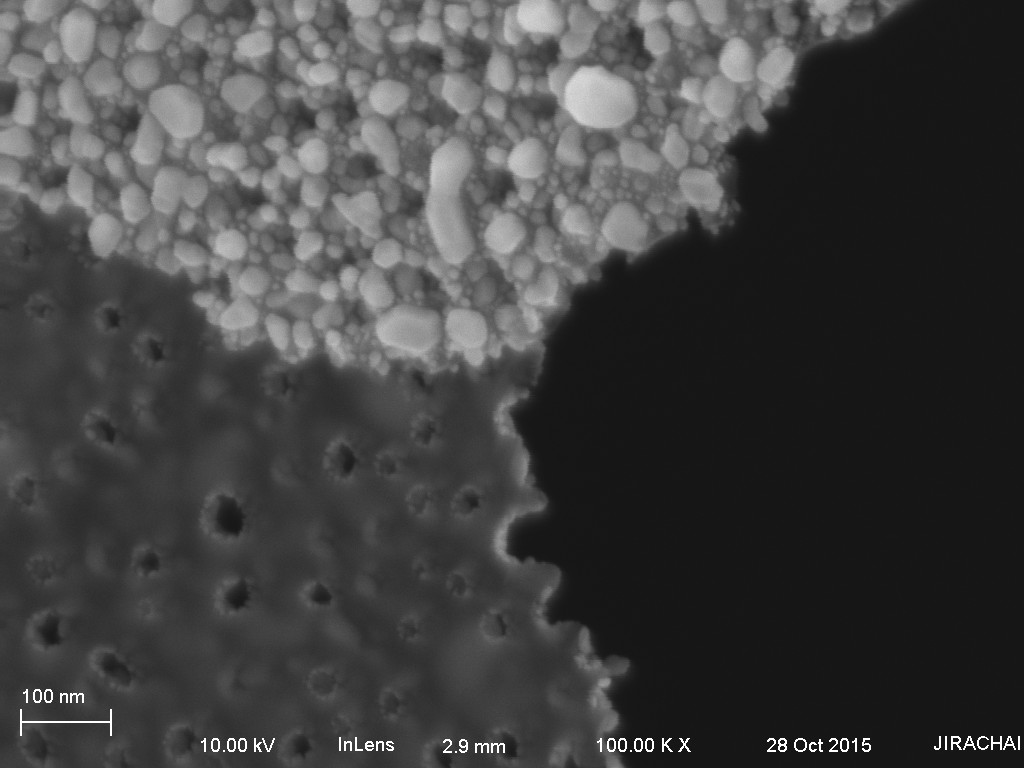
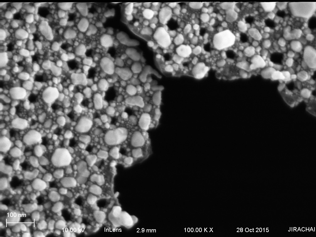
Here is a closer look on the surface of the membrane.
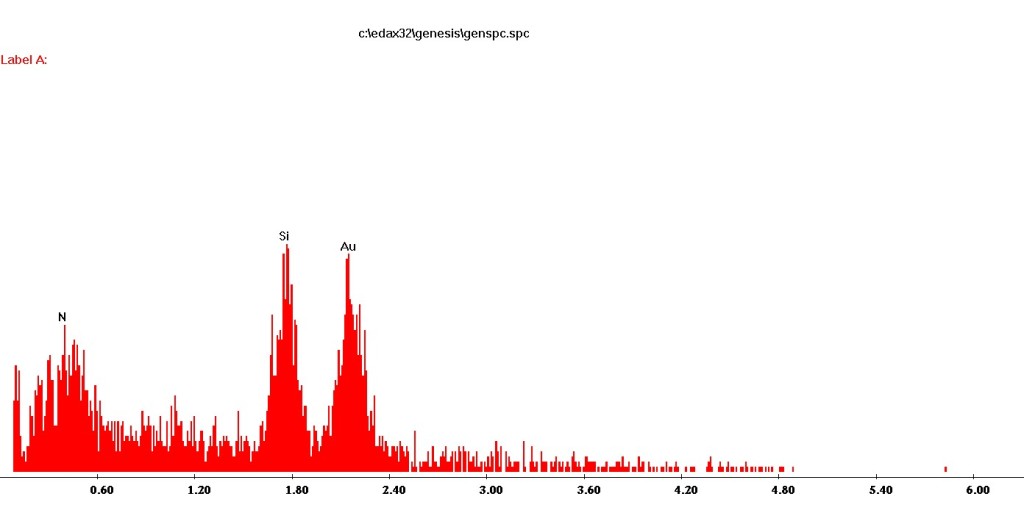
EDAX data verify that those nanoparticles on the SiN membrane are gold.
Instead of uniform coating of Au, Au nanoparticles offer much higher active surface area for functionalization, say with thiol or … Or maybe, it might be useful for other applications as well.
Method. Au nanoparticles were coated on the surface of nanoporous SiN membrane as a result of heating up the membrane at 200 C during the initial Cr evaporation and subsequent Au sputtering. The target thickness of Cr and Au was 4-5 A and 10 nm, respectively. EDAX data were obtained for the Au nanoparticles over the freestanding membrane by using low energy of 5 kV. It is expected that if EDAX data were obtained over a solid substrate and the energy was higher, Cr would be detected as well.
This is a fairly well known method for forming metal nanoparticles (I think it was even used by Josh Winans in an NRG project). Almost all metals will ball up on a dielectric film if given enough energy (heat) to be mobile. To minimize this effect, it is best to keep the substrate as cool as possible. Unfortunately, depending on the geometry of the deposition system, the plasma from the sputter process likely heats the membrane, so there may be no way to keep the membrane cool. For a smoother film, you may want to try evaporation, since the substrate can generally be kept cooler – I think Maryna metallized her samples of pnc-Si using evaporation several years ago now. Images of her films are probably buried in the blog somewhere or in one of her papers.
Nice imaging! The pattern is beautiful, as well as the even dispersal across the surface.
Could you write a little bit more about what you did for EDAX? I noticed that you did not include Cr in your EDAX image. I’m not entirely convinced the nanoparticles are pure Au. To be sure, Cr is only 5% by volume of the total film you sputtered, but I would expect it to show up based on some of the coatings that I’ve done with Ti at this thickness.
The detail of EDAX is added to the method section.