Review of nano-fabrication
Hello everyone, for my first ever post I would like to share with you a collection of ideas that has turned into a review I’ll be working on. Here you will find some selected publications that report interesting fabrication processes at the nanoscale. I have summarized the processes and added some raw schematics of how they can be adapted to better meet the needs of the group. At the very end I explore a fabrication process in the micrometer size that results interesting for groups studying cell migration through pores an how that affects nuclear rupture and repair.
Nanosphere lithography
Montagne, F., Blondiaux, N., Bojko, A., & Pugin, R. (2012). Molecular transport through nanoporous silicon nitride membranes produced from self-assembling block copolymers. Nanoscale, 4(19), 5880–6. http://doi.org/10.1039/c2nr31498c
Self-assembled block-copolymer (BCP) micelles are used as templates for creating sub-100 nm nanopores in a thin low-stress silicon nitride layer.
Synthesis of the BCP micelles: poly(styrene)-block-poly(2-vinylpyrine) copolymer (PS-b- P2VP) dissolved in in m-xylene stirred overnight at room temperature.

Summarized fabrication process:
a) Micelles were spin coated onto the substrate and exposed to Oxygen plasma to remove PS between micelles
b) Micellar pattern transfer into a-Si by SF6/C4F8 to form 75 nm (height) nanopillars
c) Highly directional e-beam evaporation of Cr layer (8 nm)
d) Wet etch of a-Si nanopillars in 40% KOH to produce Cr inverted nanopatterned mask
e) Pore transfer into SiN (100 nm) with RIE (C4F8/CH4/ He)

Transferring this process to a SiO2 based membrane should be straightforward with minor adjustments. However, control over size, spacing, and distribution of the produced pores is non-uniform over a large area.
Nanoparticles or beads could serve as an alternative to polymeric micelles to better control size and pore spacing. Some ideas are illustrated below:
Dewetting of a metallic layer is another approach to creating nanostructures that could serve as template. The dewetting process is achieved at relatively high temperatures; hence, the choice of metal/substrate must not promote diffusion. Below is an example of a Au dewetted film (depostied as a 1 nm thick layer) on an SiO2 substrate. The figure was taken from Seguini, G., Curi, J. L., Spiga, S., Tallarida, G., Wiemer, C., & Perego, M. (2014). Solid-state dewetting of ultra-thin Au films on SiO₂ and HfO₂. Nanotechnology, 25(49), 495603. http://doi.org/10.1088/0957-4484/25/49/495603:

Nanopillars lithography
Matsuu, M., Shimada, S., Masuya, K., Hirano, S., & Kuwabara, M. (2006). Formation of periodically ordered zinc oxide nanopillars in aqueous solution: An approach to photonic crystals at visible wavelengths. Advanced Materials, 18(12), 1617–1621. http://doi.org/10.1002/adma.200502383
“This paper describes a strategy for fabricating patterned ZnO nanostructures with high aspect ratios by using a wet- chemical deposition method combined with polymer molds.”
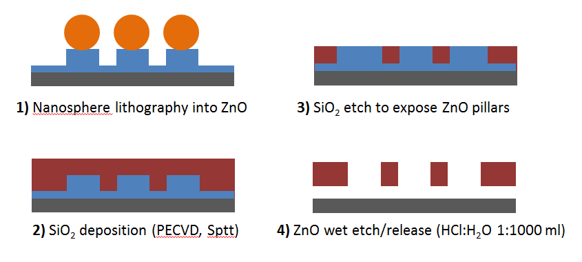
 Summarized fabrication process:
1.- ZnO “seeding” layer deposition by spin coating
2.- Fabrication of polymeric template (e-beam litho)
3.- Deposition of ZnO in aqueous solution to fill in the trenches
In the figure; a) shows a top-view of the polymeric template, b) shows a cross-section of the ZnO seeding layer and polymeric template, c) shows a top-view of the template after being filled with ZnO and d) corresponds to the cross-section showing the completely filled trenches.
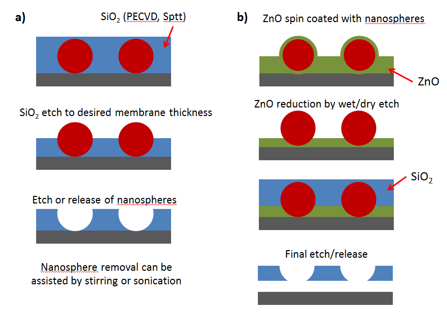
Taking advantage of the mild etchant for ZnO, a mixture of HCl:H2O 1:1000 ml, provides the potential of fabricating an SiO2 membrane if the polymeric template above mentioned is replaced by SiO2. Below is an schematic figure of how the process would proceed by the use of nanosphere litho:
Anodized aluminum oxide lithography
Lipson, A. L., Comstock, D. J., & Hersam, M. C. (2009). Nanoporous templates and membranes formed by nanosphere lithography and aluminum anodization. Small, 5(24), 2807–2811. http://doi.org/10.1002/smll.200901151
“We employ nanosphere lithography to pretexture aluminum films on a variety of substrates to create AAO films with tunable interpore spacing, pore diameter, and aspect ratio.”

Summarized fabrication process:
a) Thermal evaporation of Al layer
b) Deposition of polystyrene spheres 80, 160 and 240 nm (diameter)
c) Size reduction by Ar:O2 plasma
d) Sputtering of W layer
e) Removal of PS spheres to produce W nanopatterned mask and formation of shallow pits to serve as template for anodization (nitric and phosphoric acid)
f) Anodization of the Al layer (in phosphoric acid at 50 -150 V) and removal of W (in potassium ferricyanide)
PS spheres of 80, 160 and 240 nm produce pores with 33, 57 and 70 nm in diameter; with 84, 154 and 234 nm of interpore spacing. For the largest pore size (70 nm) the AAO thickness is up to 1000 nm. “This process has been successfully performed on glass, silicon, and silicon nitride surfaces.”
It has been shown that the anodization process can be performed on SiO2 at the expense of resulting in non-uniform depth of the trenches; however, a metallic interlayer might alliviate the issue. An AAO template with controlled geometry by nanosphere litho succesfully fabricated on SiO2, has the potential of solving the eternal limitation of anisotropy by providing a template with vertical sidewalls thick enough to allow for anisotropic etching of thicker than usual SiO2.
–Micrometer scale
Deep silicon etch – BOSCH process
The BOSCH process is widely used to create deep Si trenches with vertical walls. It can be described to be an isotropic etch made anisotropic through passivation of the sidewalls; hence, preferentially directing the etch to the bottom of the trench without the addition of Ar as typically done to increase anisotropy.
 Summarized fabrication process:
This process runs as a cycle of two short steps (<10 s each)
1.- Isotropic Si etch with SF6 plasma
2.- Sidewall passivation with C4F8
The figure below shows different trenches with the smallest width (far right) being 1.3 microns with a depth of 17 microns approximately. Figures taken from: http://robotics.eecs.berkeley.edu/~pister/147fa14/Resources/BoschProc-STS.pdf

The BOSCH process is already well studied and established; the interesting part is to design a BOSCH-like process that works for SiO2. I haven’t been able to find a reported process on this (or haven’t look hard enough), the closest approach I found was to run a typical BOSCH process and the oxidize it to make it SiO2 instead which is an idea worth exploring. Nonetheless, below you will find a schematic of a rough idea on a BOSCH-like process for SiO2:
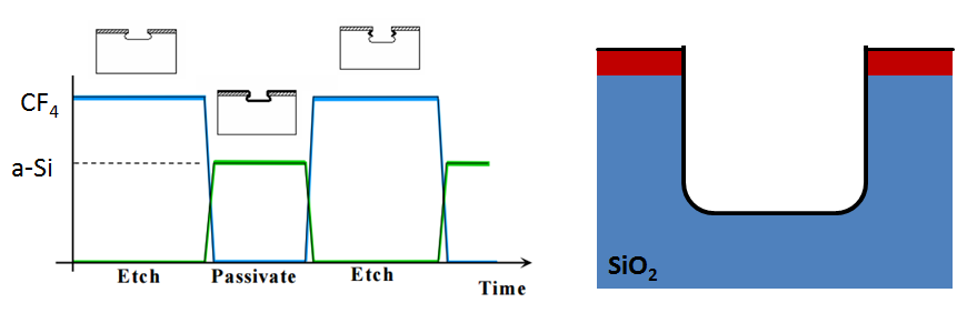
In the case pictured above, the isotropic etching step will be done with CF4 while the passivation can be a deposited a-Si layer. The etching step would have a short initial etch with high Ar flow to break through the a-Si at the bottom only. First limitation is a-Si build up on the sidewalls that can be addressed with an isotropic etch of the Si layer. Major limitation is the need of accesing gas lines of CF4, SF6 and Ar inside th PECVD tool.
I will be filling in the gaps to come up with a more detailed and feasible plan on these fabrication approaches as well as working on putting together the review.
Any comments and crazy ideas will be greatly appreaciated.