NanoAuger Analysis of Magnesium Fluoride Nanomembranes: The Hunt for Silicon Nitride
This is my third post that is related to the NanoAuger system that I had the opportunity to use while I was home over break. However, instead of quantum dots and exosomes, this time I will be talking about data pertaining to Greg’s magnesium fluoride membranes that are used for Raman imaging. And since I am not an expert in the background, I am bringing in the creator of these membranes, Greg:
YOU DON’T TELL ME WHAT TO DO!!!
WOG (Word of Greg): I have done a number of material studies of my MgF2 nanomembranes using the U of R’s EDX tool on the SEM. All have shown a 85-90% MgF2 signature with some silicon remaining. Being that the nanomembranes are so thin, most of the EDX signal passes straight through the nanomembrane and it takes a long time to measure anything effectively (to counter this effect, I’ve previously folded pieces of membrane on itself to increase the crossectional area. Other measurements from Josh Winans’ XPS era suggested that the silicon was not in the volume of the MgF2, but underneath as a scum layer, from incomplete etching, but I have been unable to confirm it. I can bound the layer as less than 5 nm based on the SEMs that I have made, but direct verification would be better.
With that background, we can now jump into the data. When I started off with running these samples, we initially took EDX maps and spectra to show the capabilities of the system. Fig. 1 shows the EDX data from the freestanding membrane:
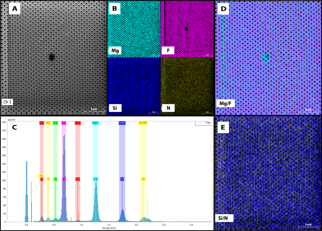
Figure 1: NanoAuger EDX Data for magnesium fluoride membranes. A) SEM image of sample surface taken with the NanoAuger. B) Individual elemental maps of the membrane. C) EDX spectra of the membrane. Note how the magnesium and fluorine peaks are larger than the silicon and nitrogen. Also note the copper signal. D) Overlay map of magnesium and fluorine. E) Overlay map of silicon and nitrogen.
As I stated in a previous post, EDX is probably one of the worst ways to try and get elemental information from our freestanding membranes. Because of the depth of penetration for the beam and the large sampling volume, the data is often not sensitive enough for very thin layers. However, with this data, there are a few good points that we should note. First off, we are able to pick up that there is a silicon nitride layer underneath the magnesium fluoride membrane. This is great, as Greg has already shown this with the system at U of R. However, there was also a small copper signal that we did not notice until running the Auger analysis, so we labeled it on the spectra after seeing that. One other feature to note is in the maps themselves. These are 1024 x 1024 resolution maps, so that means we can distinguish the individual pores in the mapping as well as the imaging (these are microporous membranes with ~400 nm pores). This is a very nice feature which plays into the next data set.
(WOG): Copper is concerning for a number of reasons; it can be poisonous to cells, and it can be very damaging to semiconductor devices. If there is residual copper in the evaporator from URnano, that is important to anyone who is trying to make very pure films. The most likely source is that my crucible became contaminated, which we can change out. If it is somewhere else in the tool, which can happen from time to time, it is unlikely that we can do anything about it, other than requesting the tool to be cleaned and baked, which may not fix the problem.
After analyzing the membrane, I decided to move to the non-freestanding region so as to get baseline measurements for what the substrate looks like as an EDX spectra. As we can see in Fig. 2, the distribution of the signal is quite different, which we would expect:
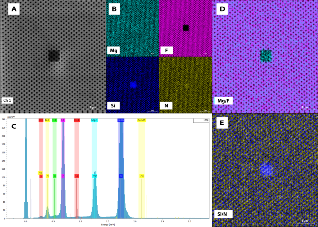
Figure 2: NanoAuger EDX Data for magnesium fluoride on the substrate. A) SEM image of sample surface taken with the NanoAuger. B) Individual elemental maps of the membrane. C) EDX spectra of the membrane. Note the change in the silicon signal from Fig. 1. D) Overlay map of magnesium and fluorine. E) Overlay map of silicon and nitrogen. Note how the silicon is distributed at the bottom of the holes.
Figure 2 shows us that there is a much larger silicon signal than can be seen in Figure 1, which we know should be true because the region analyzed is not freestanding. This is a good baseline check for telling whether or not we have silicon nitride at the bottom of the membranes. One feature to note in Figure 2 is the beam burn that is evident at the center of the sampling area. We were working with a 10 keV beam, so at a higher magnification it burned the surface a small bit.
While the EDX data is quite good, it is really only a confirmation of data that Greg already has, so we then switched the system over to Auger mode and started to get more into the nitty-gritty of the sample. We took an initial spectra of the surface and it showed only what we expected, which was magnesium, fluorine, carbon and oxygen. Silicon and nitrogen are nowhere to be found, because they are not present in the surface of the membrane. This was actually a slight problem as our next step was to set up a depth profile and in order to do that, you typically select a very specific area around a peak on a spectra with your element of interest. However, we had to use the system default for silicon and nitrogen in this case since they did not show up in the spectra. We were quite lucky and there was no peak shifting, so the regions that we selected encompassed the peaks for silicon and nitrogen.

Figure 3: Auger spectra of the magnesium fluoride membrane before sputtering.
Before I present this data, I will briefly describe the procedure for a depth profile in an Auger or XPS system. Basically, the goal is to ablate the surface and then trace the signal of the elements at each ablation step. Typically, these systems are equipped with argon guns that are very gentle (FIB beams are gallium, which is quite aggressive) and can remove the surface very slowly. The system voltage can be adjusted as well, creating highly sensitive layer removal for thin films. Typically, when running a sample we choose to sputter at a rate of 1 nm/min so that we are going quite slowly through the sample. In the case of these samples, I believed them to be 50 nm thick membranes, so we chose to sputter at this rate. This means that the system would take an initial spectra for each element selected (in this case magnesium, fluorine, silicon, nitrogen and gold) and then sputter the surface for a total of 1 minute and then cycle through this process of taking spectra and sputtering. The data is then plotted as intensities, but can be converted into atomic concentrations.

Figure 4: Full depth profile of the magnesium fluoride membranes. The red dashed line indicates where we switched to a faster sputter rate. At approximately a depth of 130 nm, we can see an increase above baseline for silicon and nitrogen.
Fully expecting that these membranes were 50 nm thick, we came back after lunch to find that there was really no change in the data and there wasn’t really a decrease in the intensities of the magnesium and fluorine peaks. Additionally, there was no silicon or nitrogen signal coming through. This was very puzzling and I had to call Greg to ask why this may be. He then proceeded to inform me that the membranes were not 50 nm thick, but in fact they were 200 nm thick. Which meant that it would take well over 200 minutes at the rate which we were sputtering to get anywhere near the bottom of the membrane. This was not really feasible, especially as instrument time is quite expensive so we decided to increase the sputter rate to 6 nm/min and sputter at 2 minute intervals. This means that we would remove approximately 12 nm between each layer of analysis. So we sacrificed some resolution for getting to the bottom of the membrane, but this wasn’t really terribly much in the long run. Right before we started the depth profile, we took another full spectra, which again showed us something quite strange: a copper peak set had appeared in the spectra. If you remember from earlier, I noted a copper signal in the EDX spectra on the membranes. Well, this is how we knew to label the copper in that spectra. I immediately thought that this could come from contamination in the system, but there was no copper present so Greg’s hypothesis is that due to its location in the membrane (in the bulk, rather than in the surface) the copper comes from the manufacturing process and contamination in his crucible.
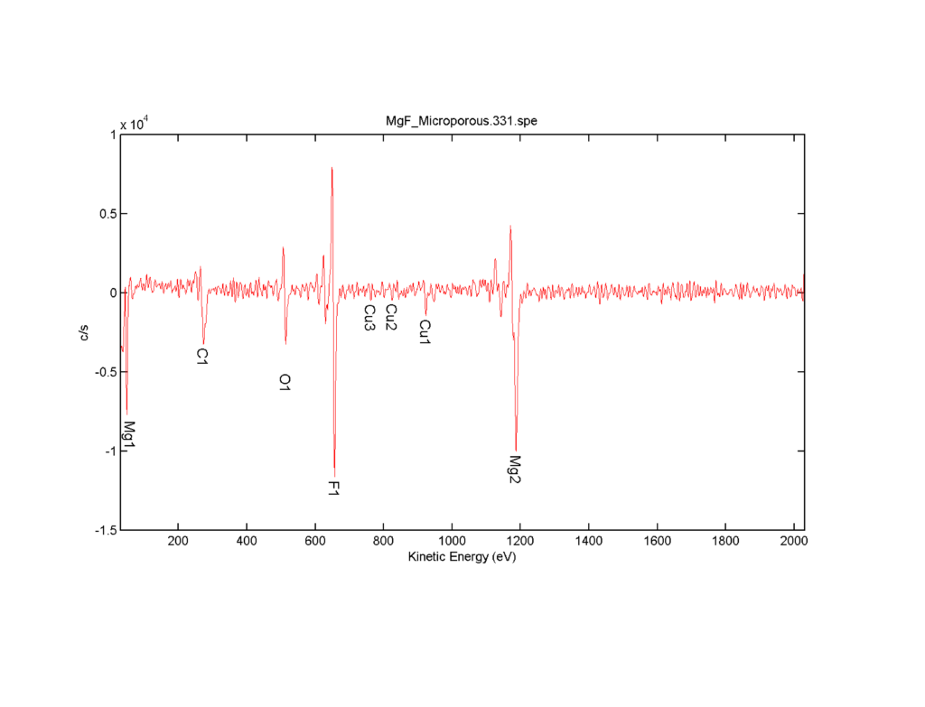
Figure 5: Auger spectra from the middle of the membrane. Note that there is a copper peak triplet present, but still no silicon or nitrogen.
With this new spectra and still no signal from silicon or nitrogen, we restarted the depth profile, which now ran significantly faster. If we now go back to Figure 4, we can look at the data and notice something that is actually pretty remarkable. I didn’t notice this until I was compiling the data into the figure, but the end of the first depth profile exactly corresponds with the start of the second depth profile. This is even after the data was converted from intensity to atomic concentration. Basically, we completely stopped the system, messed around with imaging and taking spectra and then changed some parameters, but the analysis wasn’t affected by this. This was really nice because it meant that I could merge the two profiles and not have it be cheating in any way.
Eventually, we stopped the depth profile, more due to a time constraint than anything else. What we noticed was that we were approximately 280 nm through the sample, but the membrane was only supposed to be 200 nm thick. The reason that we do no see a complete loss of signal from magnesium and fluorine is likely due to the toughness of these materials and the relative weakness of the sputtering beam. If we had run the sample for longer, we would have been able to get completely through the membrane, but that is probably a good idea for a future data set. However, to show that we were indeed at the bottom of the membrane, we took one last spectra and at this point we can see silicon and nitrogen present:
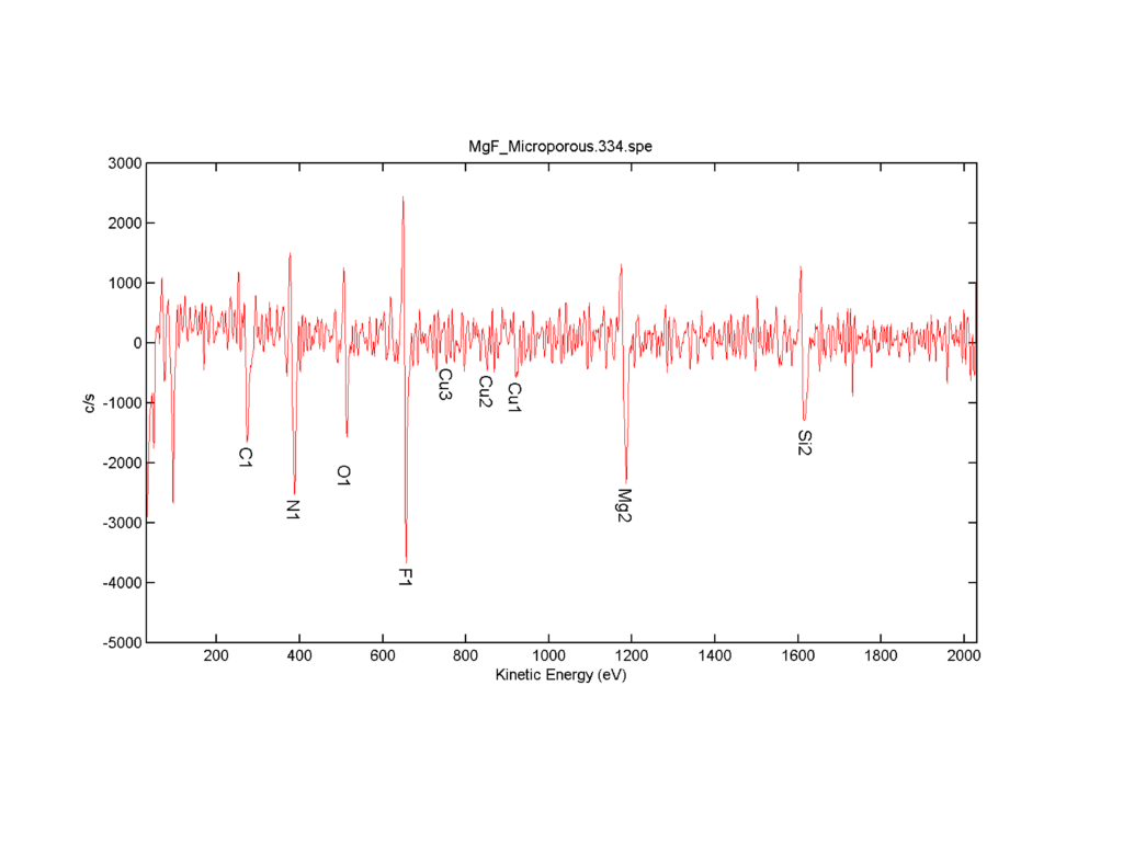
Figure 6: Auger spectra after full depth profile. Note now how we see silicon and nitrogen, which are on the bottom of the membrane.
At this point, we pretty much had reached the end of the day for using the instrument. However, the data was quite useful. In comparing this data to the EDX data that either Greg or I took, we can see that there is much more sensitivity that is available with the NanoAuger system. As it stands right now, where we would like to go next with this experiment is to perhaps obtain a higher resolution depth profile, where we sputter fast through the magnesium layer and then as we approach the silicon nitride at the bottom, we could slow down and more carefully analyze this region. This would allow us to obtain a more precise value for the thickness of the silicon nitride layer on the bottom of the membrane. Additionally, if we took one of Greg’s membranes with the gold volcanos on it, we could do high resolution depth profiling of the volcanos and also incorporate Auger mapping of the surface, which would be similar to an EDX map, but again would be more sensitive to the surface. Basically, this tool has provided us with some nice data and has opened the door to other questions that we may have not been able to answer with what we previously had available to us.