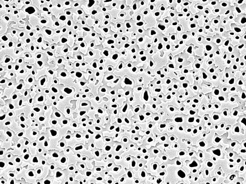
Where oh Where can the holes in my 75 nm Membranes be?
Another set of images of both sides of a membrane, this time something weird is happening… It looks as though I’m missing some holes from the top side. They looked to be filled in but are not when seen from the back.
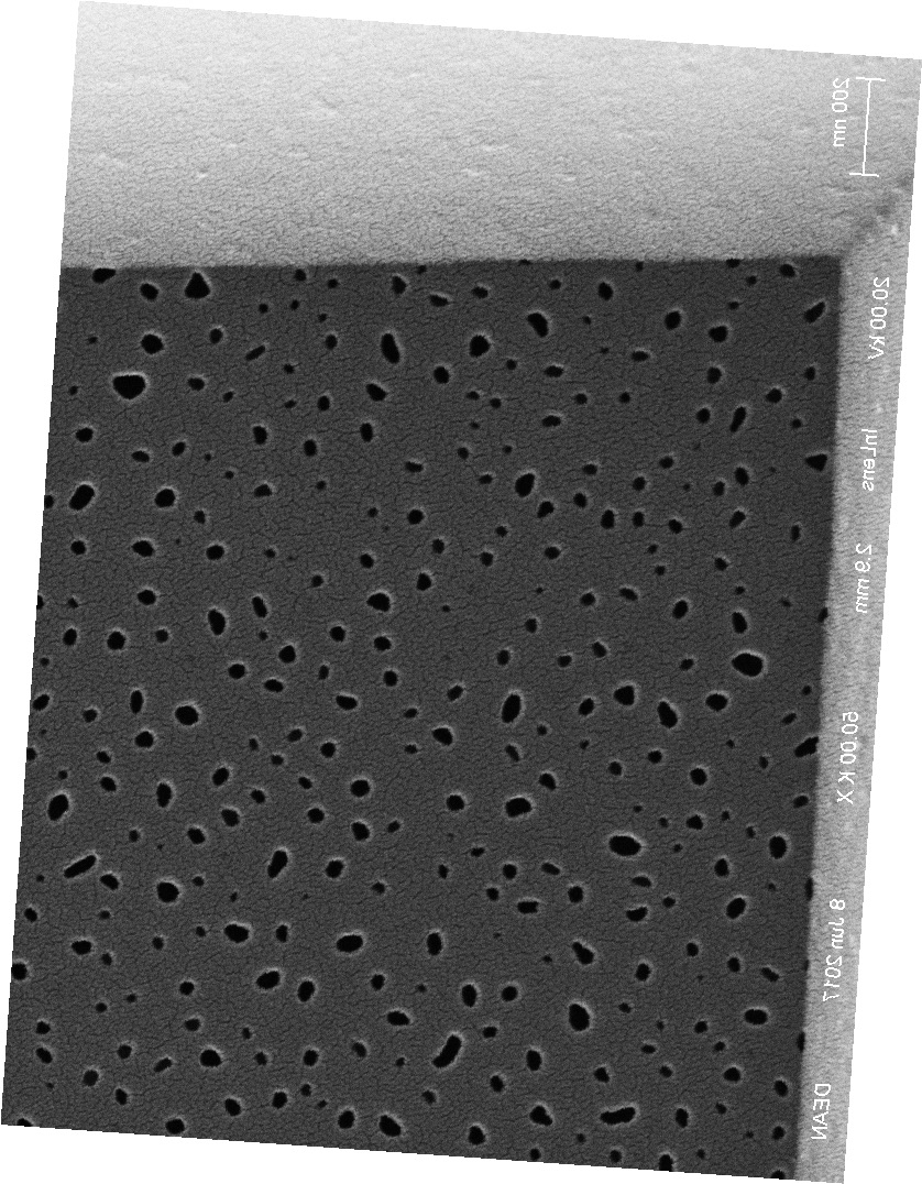
Here is the backside of the wafer showing a bunch of holes. (the image has been rotated and flipped to match the top side orientation)
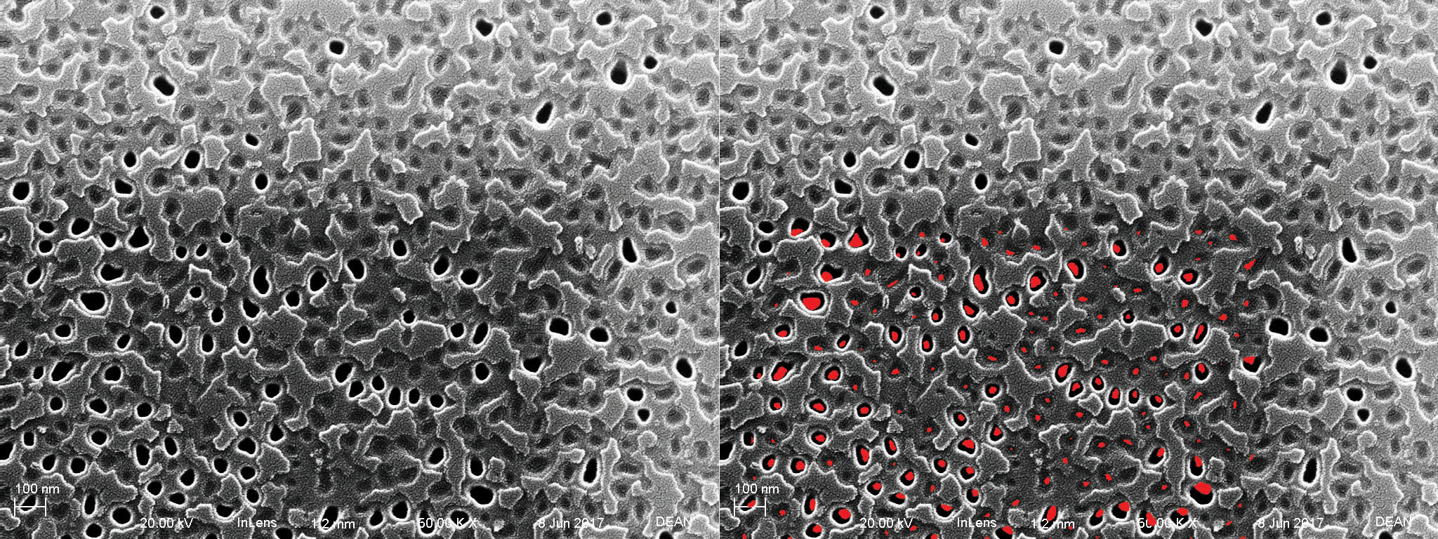
Here is the top of the same corner with and without the overlaid holes (in red) from the bottom. Clearly you can see holes where on the topside there seems to be no through hole.
I my Gold-Palladium coating (40 s) thick enough to span the gap? I wasn’t very pleased with the images on the backside of this wafer and will be redoing the SEM on Tuesday.
I did notice that this appeared near the edges, or more precisely the corners, of the membrane area. I’m wondering if it could be an affect of the trench etching since the pores must have gone all the way through the membrane to appear on the backside. Does anyone else image near the edge of the bulk silicon? Just a thought. Also, I coated the topside, imaged it, then flipped the chip, recoated and imaged the backside, so if any pores are getting a double dose of gold-palladium, its the pores in the backside image, so it seems unlikely to me to be caused by the coating.