Manufacture waveguides across porous nanomembrane: a new biosensor
Abstract:
In this project, we want to explore the possibility of detecting molecules in nanopores by building waveguides upon a silicon nanomembrane chip. The first experiment is performed by sending 650nm laser light onto our waveguides and detecting the light waveguided by our patterned structure. This is used to prove that light can overcome the scattering and absorption along the waveguides and still provide enough signal we can detect. The next several experiments will be about quantifying the loss of light across the nanomembranes and other related parameters. The possible application of this biosensor may be imaging the fluorescence of the exosomes trapped in the pores on the nanomembrane.
Methods:
The process of manufacturing waveguides across the nanomembrane has been found and successfully implemented by using SU-8 photoresist spin coating.
First, we select the correct size of chip holder for our silicon nanomembrane chip and spin coat it with SU-8 2000.5 photoresist with initiator. The resultant thickness of the photoresist layer is approximately 450nm:
After that, we soft bake for 60 seconds at 95 Celsius degree. Then we use Microtech Laser writer to pattern the waveguides on the spin-coated nanomembrane chip. The setting for the Laser writer is lens 4, 30% filter and 450mj/cm^2 exposure power. The chip must be well aligned and highly focused to perform a successful patterning. After post-exposure bake for 3 and half minutes at 95 Celsius degree, we develop the patterned chip for 4 minutes and wash it with IPA for another 2 minutes. Then the chip should be carefully dried and hard bake for 10 minutes at 120 Celsius degree.
Later on, a cladding layer is recommended on the top of the waveguides layer, because it can prevent scattering of the light out of the plane. Then the loss can be decreased and it is easier to see detect the signals.
The following are few different types of waveguide samples I manufactured without the cladding layer.
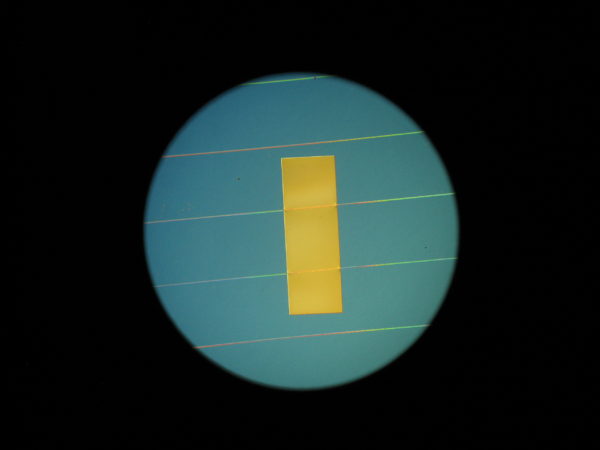
Figure 1: DIC image of the straight waveguides across the nanomembrane chip.
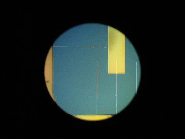
Figure 2: DIC image of the L shape waveguides across the nanomembrane chip.
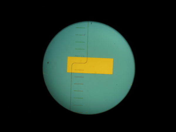
Figure 3: DIC image of the S shape waveguides across the nanomembrane chip.
Problems:
There are some problems relating to the quality of the waveguides. The following is an image of the disjointed waveguide at the intersection between the membrane and the silicon substrate.
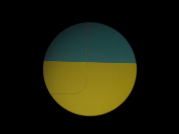
Figure 4: DIC image of the disjointed waveguides across the nanomembrane chip.
The possible reasons for this phenomenon will be the insufficient exposure under the laser writer. I already fixed this problem by adjusting the appropriate range of exposure rate (450~460mj/cm^2). The focus of the objective lens in the laser writer is also important for a good quality waveguide.
Besides the disjointed problem, there is also defect appeared at the intersection, shown in the following image:
Figure 5: DIC image of the defect on the waveguide at the intersection between membrane and substrate.
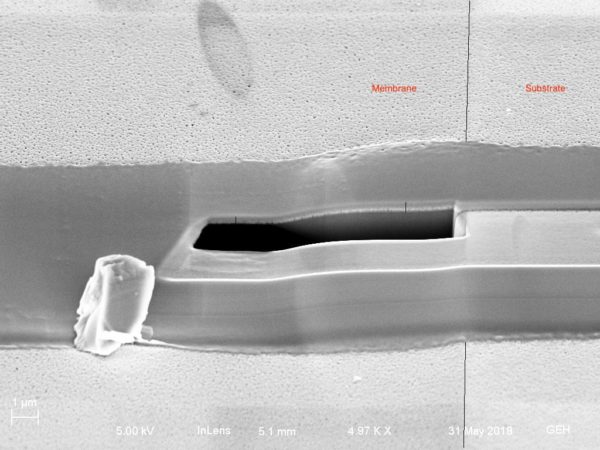
Figure 6: Focused Ion Beam cut on the intersection between the substrate and the membrane.
From the picture, the thickness of the waveguide on the membrane side adjacent to the intersection is much larger than other thickness of the waveguide before or after the intersection. This might cause great loss of light and I still couldn’t figure out a way to avoid this.
System setup and experiment:

Figure 7: system configuration. A DIC microscope is used to monitor the input and output fiber alignment with the sample. The input is a 638nm ~ 650nm laser diode connecting to a fiber emitter. A power meter is used to quantify the output power received from the fiber receptor.
The sample I tested was the straight waveguide lens pattern. The laser diode has a power of 30mW, and the output power I detected from the waveguide is 2uW maximum. I didn’t measure the power emitted from the fiber, but I believe the input/output ratio will not be larger than 30mW/2uW. However, the main challenge here is to prove that the detected light is from the waveguide but not directly from the input fiber emitter. I used two methods to approach this.
First, align the input fiber emitter, the waveguide, and the fiber receptor. Move the sample stage horizontally so that the waveguide is not aligned with fiber emitter and fiber receptor anymore, but the emitter and receptor are still aligned with each other, as shown in the figure below:

In such way, if the power reading drops significantly, we can prove that waveguide is coupling light into the fiber emitter. However, I just tried this method yesterday and it failed. The output power almost remained the same at around 1.2uW when the light was not tunneling through the waveguide.
Then I tried the second method. This time I also aligned these three components, but instead of moving sample stage horizontally, I moved the sample stage vertically downward, such that there was nothing in between the emitter and the receptor. Interestingly, the power meter reading dropped significantly as soon as I leveled down the sample stage. This phenomenon somewhat encouraged me.
After that, I have tried to send light into a waveguide which has a huge defect in the middle, the power meter reading was as small as few nanowatts. From the first method, we know that the receptor can also detect light when the waveguide is misaligned. But this time we cannot detect light from a flawed waveguide. The most likely reason for that is light was scattered by the defect in the waveguide, which proves that light can be sent into and out of the waveguide. But this process is so lossy that cannot be differentiated from directly walking across the substrate.