Lift-off Attempts for a Bone-Invasion Mimetic with Porous Roof using 100 nm NPN
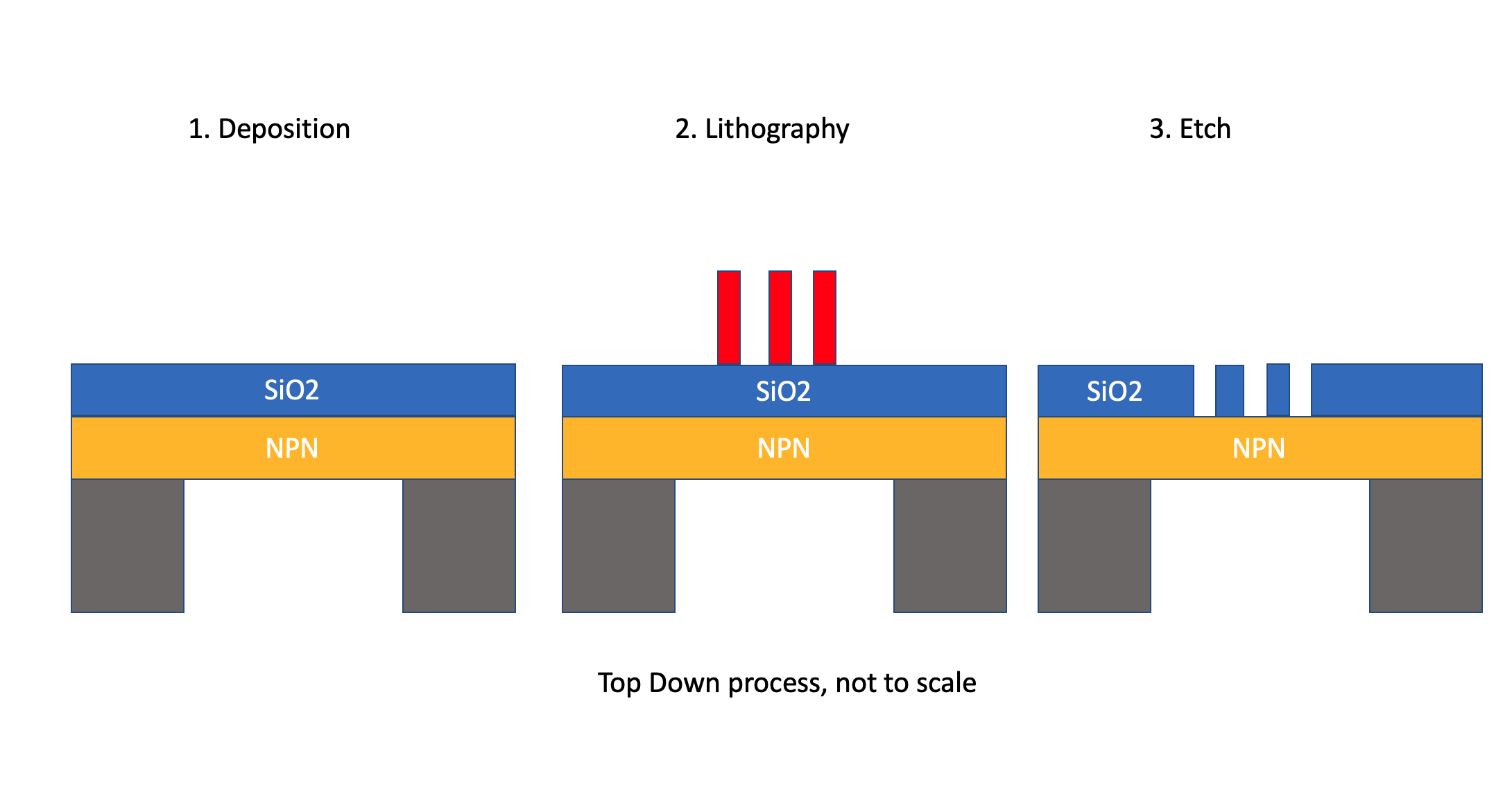
This post is a continuation of the project found here: Fabricating 500 nm Channels in Silicon Wafers. The chief limitation of the previous device design was that the long narrow nanochannels were not effectively wetted. To combat this problem, we would like to fabricate the channels in situ on top of NPN. This could be accomplished with either a bottom up approach (lift-off) or a top down strategy (sputter/litho/etch). I chose to try the lift-off process first, as it would not appreciably change the NPN layer.
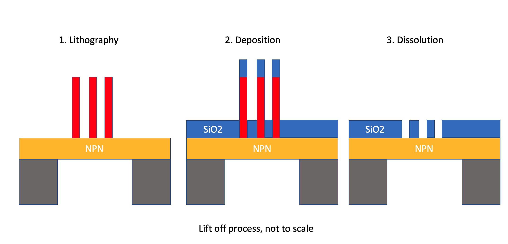
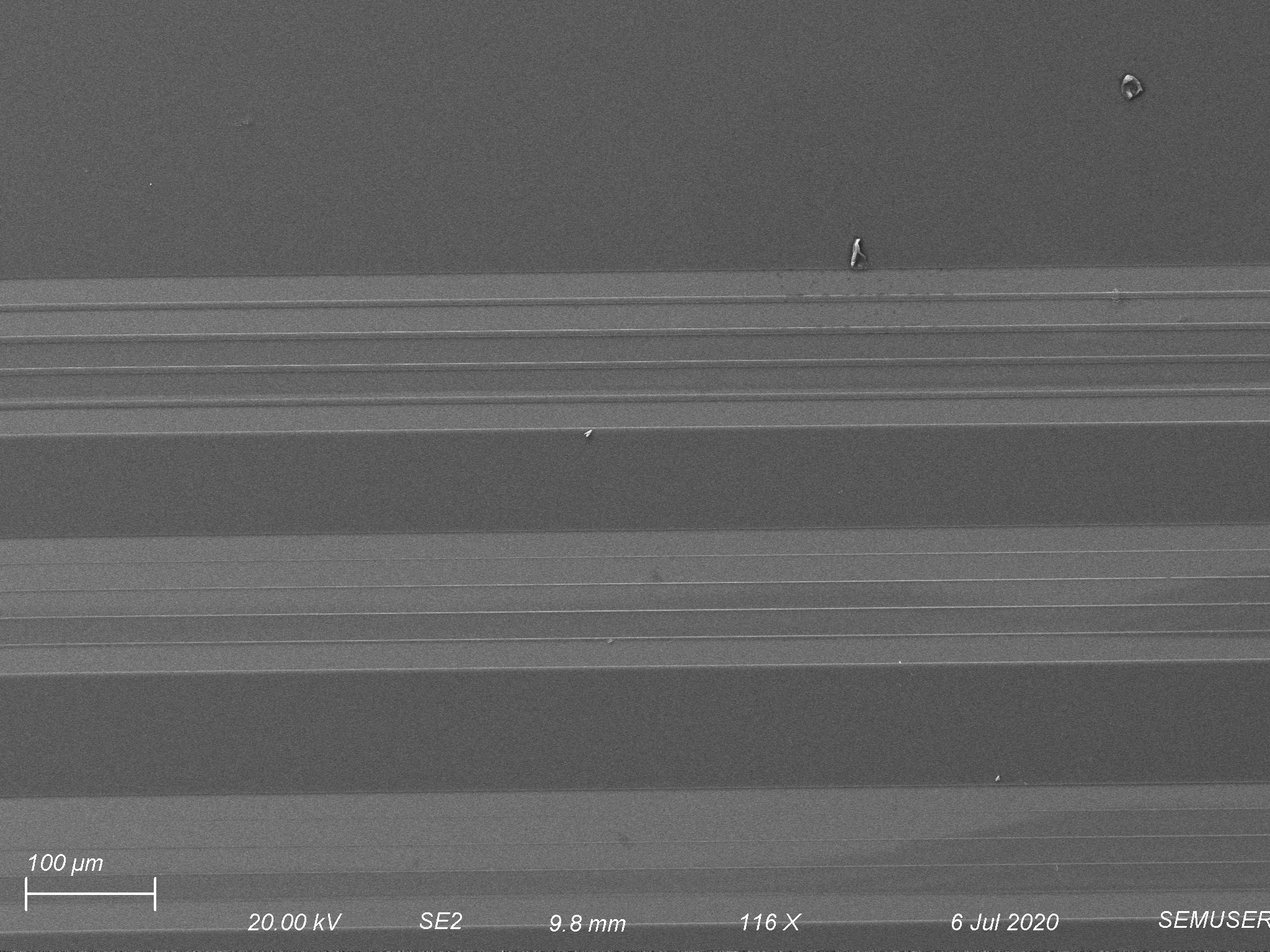
The photoresist that we have been using with the laserwriter is S1805, which has the necessary resolution to get down to 500 nm wide channels, however, it may not be able to get thick enough to perform good lift off. S1813 resist can be layered on twice as thick, but it is unknown if the laserwriter will work with this resist (It might not have the right dye sensitizer). Both of these resists are positive-tone, meaning that an exposure of the right light energy will cause the resist to dissolve in developer solution (SU8 is a counter example as a negative tone resist, which solidifies with exposure to light energy), so in order to create the channel void, two precisely positioned laser paths must be written with only a 500 nm gap between them. Some work has been done a few years ago to do lift-off processing with SU8 for Josh Miller’s Sr Design project (SU8 lift-off characterization, Feasability of SU8 3010 Negative Resist for Lift-off., Nano-porous SiN Lift-off with SU8 3010 Negative Resist).
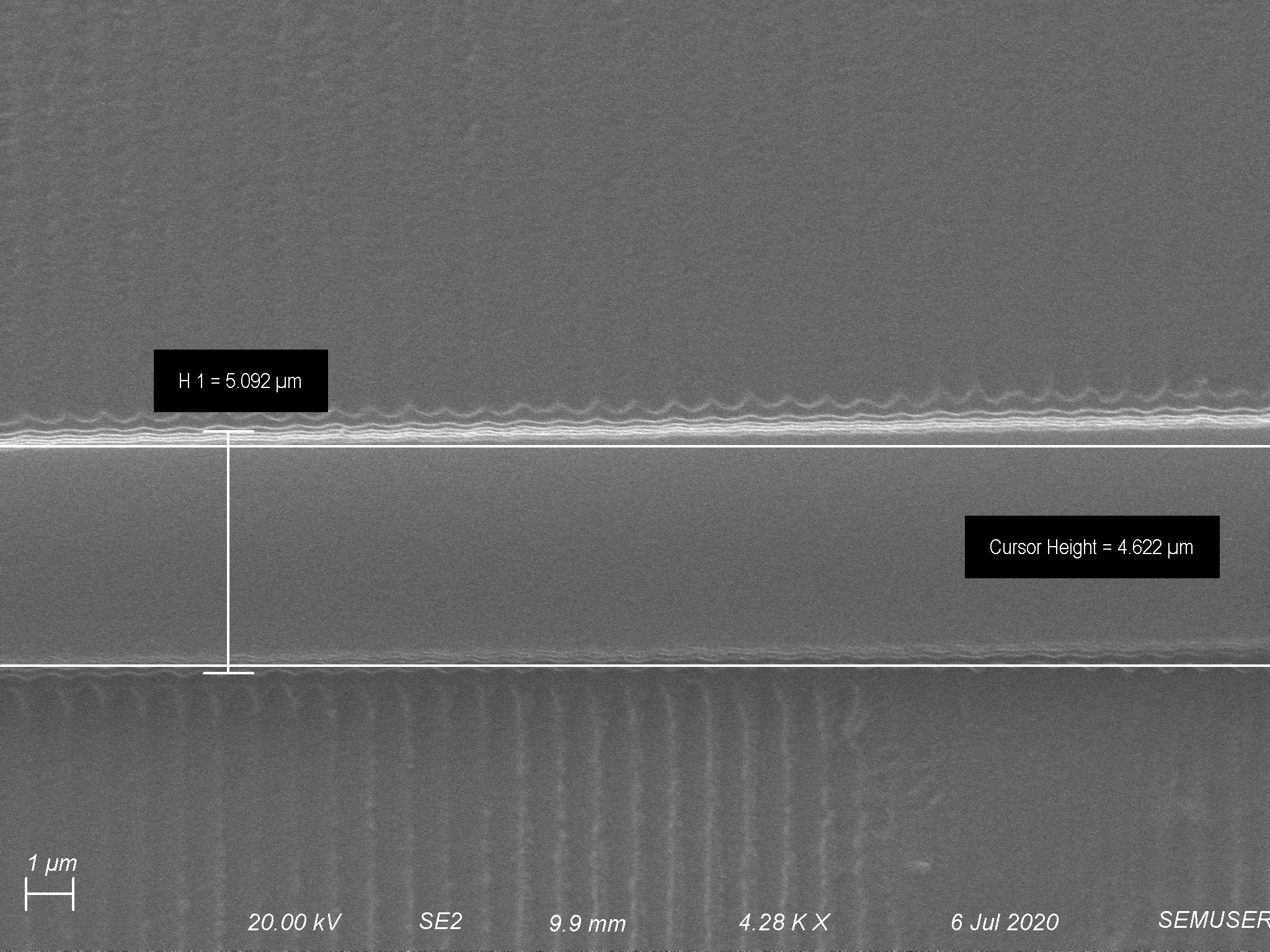
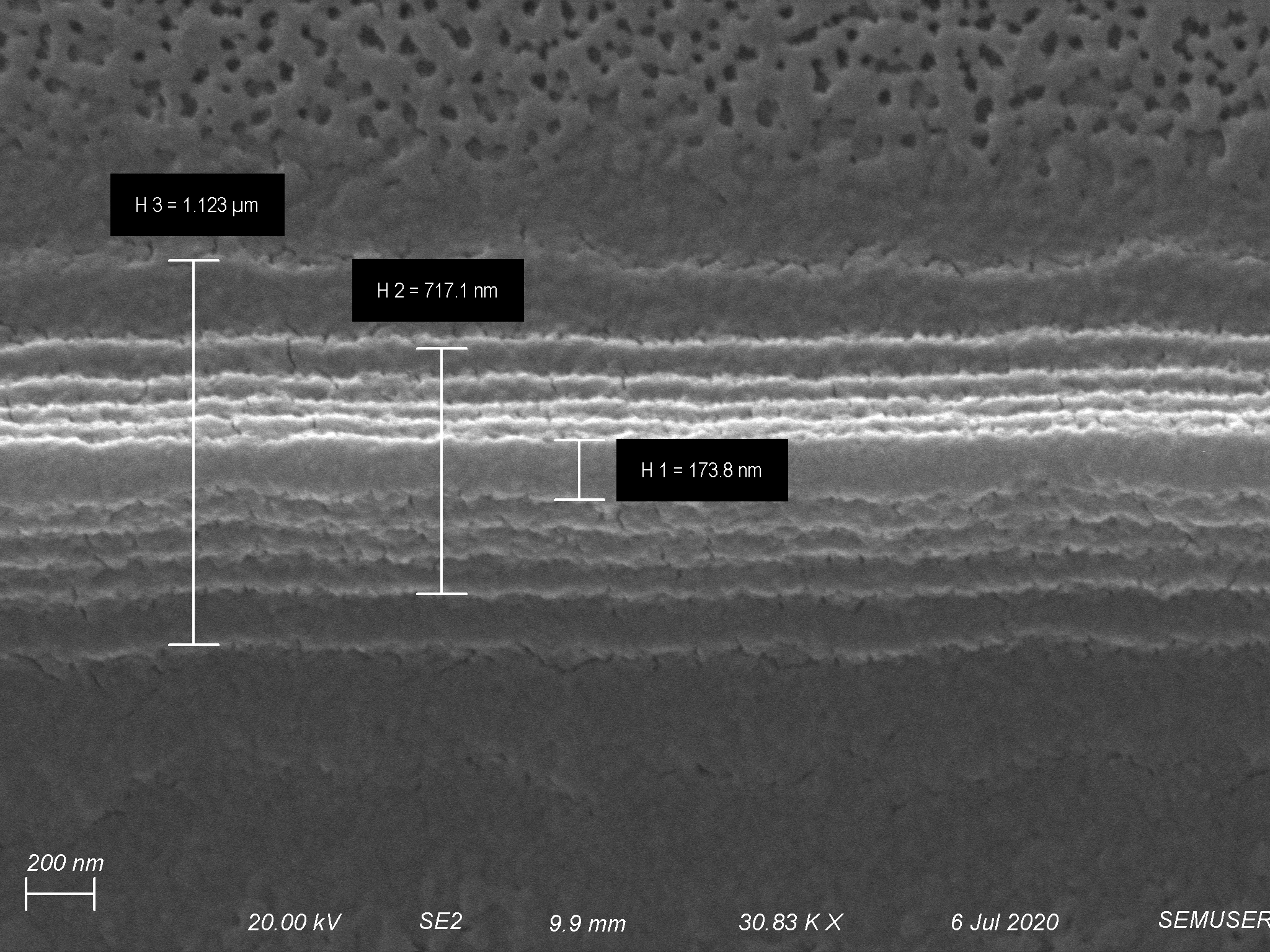
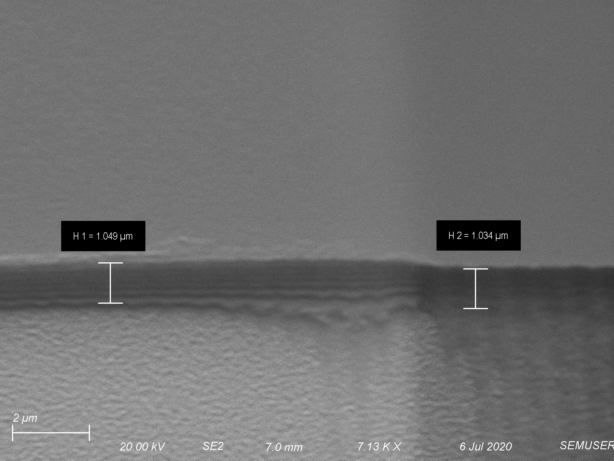
As S1805 will not coat to a thickness to reliably lift off the deposited films, I will have to switch to S1813 or Su8, which will have different patterning parameters. Creating excellent sharp patterns on the resist is necessary for the lift-off process to work well.