100nm thick pnc-Si membrane
From the past experiments we know that it is not easy to form pores in thicker silicon layer. It is mainly because that higher energy is required to form open holes in a thicker silicon film. Dave showed us less but bigger pores were formed in a 50nm thick silicon film after annealing. According to this result, it is expected that open pores are less likely to form in a 100nm thick silicon film after annealing. The samples I test are OSO and NSN stacks with 100nm thick silicon layer and 30nm thick oxide and nitride layers. The annealing temperature is 1000C and ramp rate is 50C/s. Both samples are annealing for 1 minute. The followings are the TEM images of both sample after annealing.
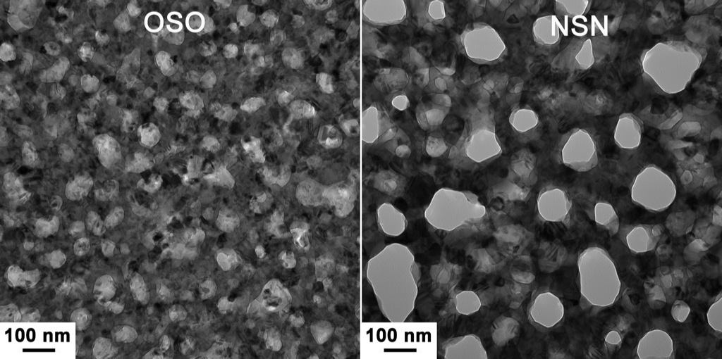
The TEM image of OSO stack clear shows that open pores are barely formed after annealing and the dominant feature is unopened holes, or pits in the silicon film, which is what we expect. On the contrary, lots of very big open pores are formed in silicon film from NSN stack and the pore. The porosity is even as high as around 17.5% with an average pore diameter around 96nm. This is first time to achieve pnc-Si membranes with very high porosity as well as such big pore sizes. The silicon crystal sizes from NSN stack also are bigger than those from OSO stack and it is in accord with our previous results.
This new result from 100nm thick pnc-Si membrane further proves that silicon nitride layers are prompt to the silicon crystallization and thus is a better material to help silicon film to form more and bigger pores.