SU8 lift-off characterization
| Etch Rate in BOE 10:1 | Thermal Oxide |
TEOS PECVD Oxide |
LTO Sputtered |
|
10:1 BOE at 20C |
66 nm/min |
266.4 nm/min |
> 180 nm/min * |
Each oxide type was placed in BOE w/ surfactant for 10 seconds, then the rate per minute was determined. *after 10 seconds no oxide remained on LTO sample therefore the exact rate could not be determined.
Based on these rates, a ten micron SU8 line should take 76 minutes (assuming an equal etch from both sides) for thermal oxide, and 19 minutes for TEOS. These are best case scenarios, no effect of thin channels and sequestering of the BOE under SU8 line. Contrary to what is expected, The SU8-SiN structure lifted off 25nm of thermal oxide in 25-30 minutes in previous lift-off attempts. To examine this closer, Wafers with SU8 over TEOS have been etched at different durations, dried and examined under the microscope. What is observed is the under etch of the oxide residing below the SU8.
Two thicknesses were chosen for the oxide: 25 and 150 nm, the same that will be used for lift-off experiments when the wafers come back with SiN. Two line widths were chosen, 10 and 5 microns for the SU8 over the oxide. A sample of each was suspended partially in BOE 10:1 with surfactant for various amounts of time. Each sample was then examined to determine the rate of undercutting. At 5 minutes there should have been approximately 1.25um from each side missing due to under etch after the windows cleared. At 10 minutes: 2.5 microns, and so on.
Results: The actual etch rate appears to be significantly faster, up to 2x faster than expected, see the following images. After measuring the samples, I have determined that the masks are quite far from spec, but this has not caused any problems yet. The actual dimensions are as follows: 5 um with 50 um openings are actually 7.5-10 um with ~45um windows for a total line-space size of ~55um (target) with a longest diagonal distance of 17.7 um. For the 10um and 100 um space: 15um lines with ~95um spaces for a total line-space size of ~110 (target) with a longest diagonal distance of 22.3 um. From these results it appears that there may have been a problem with the way the features were repeated across the mask design, but this should not adversely affect the outcome.
Given that the lines are thicker than expected, means that the etch rate under the SU8 is faster yet, given that it has ~5 more microns in the 10um case than previously expected. This may be due to exposure on oxide vs. Silicon.
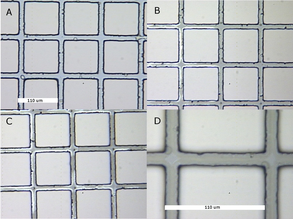
A) 25nm oxide with 10um lines before etching. B) 25nm oxide with 10um lines after 5 min in BOE. The left side was in BOE, the right side was not. This is the BOE-air boundary. C) 25nm oxide with 10um lines after 5 min in BOE. This is a section of fully submerged SU8, the ‘white’ regions appear to be SU8 without oxide under them, but there is also large areas of fully intact oxide under the SU8 (dark regions). D) 25nm oxide with 10um lines after 10 min in BOE. Here is an enlarged image (50x) of the 25nm oxide, this time the oxide appears under the SU8 only at the intersection. This did not release, so I conclude that those are likely holding the SU8 to the wafer. After 20 minutes, it appears the SU8 is clamped to the wafer and did not lift off (no picture).
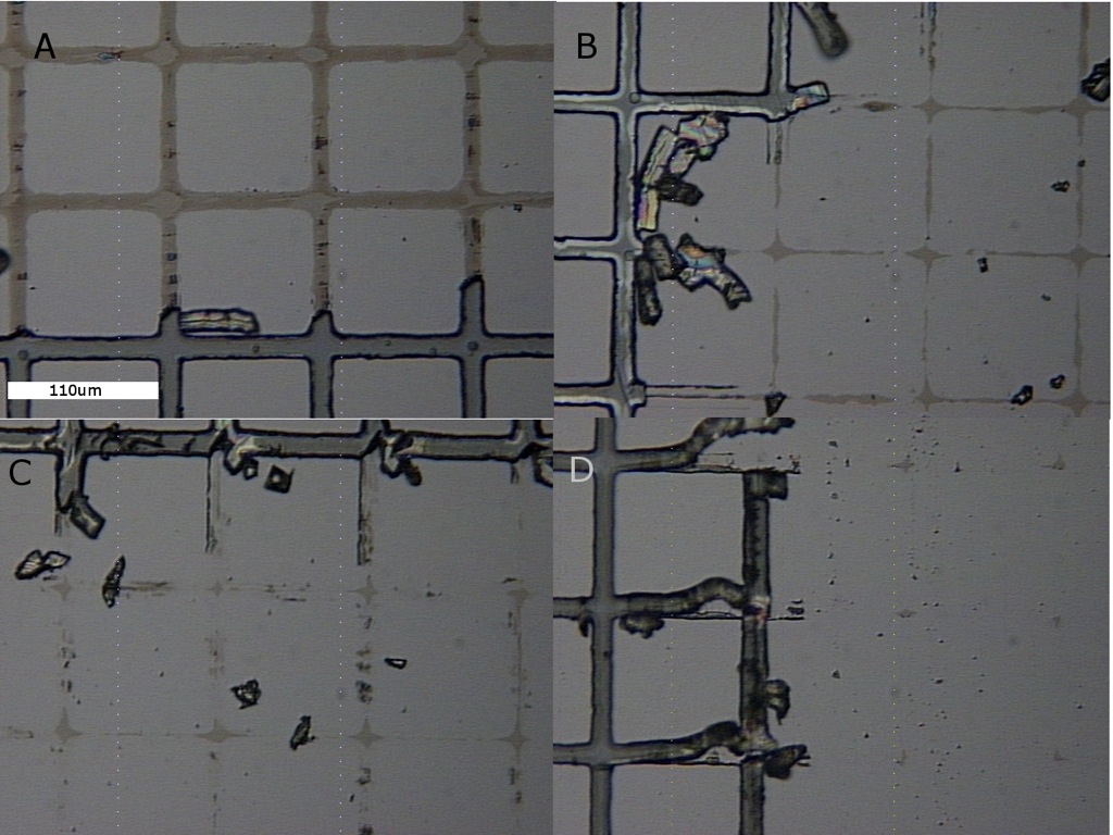
A) 25nm oxide with 10um lines after 2.5 min in BOE. Here the SU8 has been scratched off the top portion to reveal the oxide. B) 25nm oxide with 10um lines after 5 min in BOE. Here the SU8 has been scratched off the top portion to reveal the oxide. C) 25nm oxide with 10um lines after 8 min in BOE. Here the SU8 has been scratched off the bottom portion to reveal the oxide. D) 25nm oxide with 10um lines after 10 min in BOE. The only oxide remaining is that under the ‘t’ as expected from Image C in the previous set.
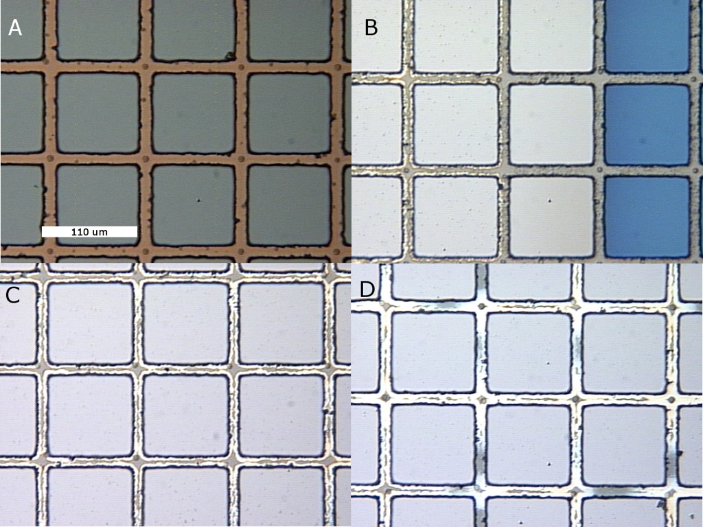
A) 150nm oxide with 10um lines before etching. B) 150nm oxide with 10um lines after 5 min in BOE. The left side was in BOE, the right side was not. This is the BOE-air boundary. C) 150nm oxide with 10um lines after 5 min in BOE. At this thickness, the under etch is much more uniform across the submerged portion of the sample than it was for the 25nm oxide. D) 150nm oxide with 10um lines after 7.5 min in BOE. Oxide is nearly gone the solid dark regions are believed to be SU8 in contact with the substrate, at 10 minutes no oxide was left.
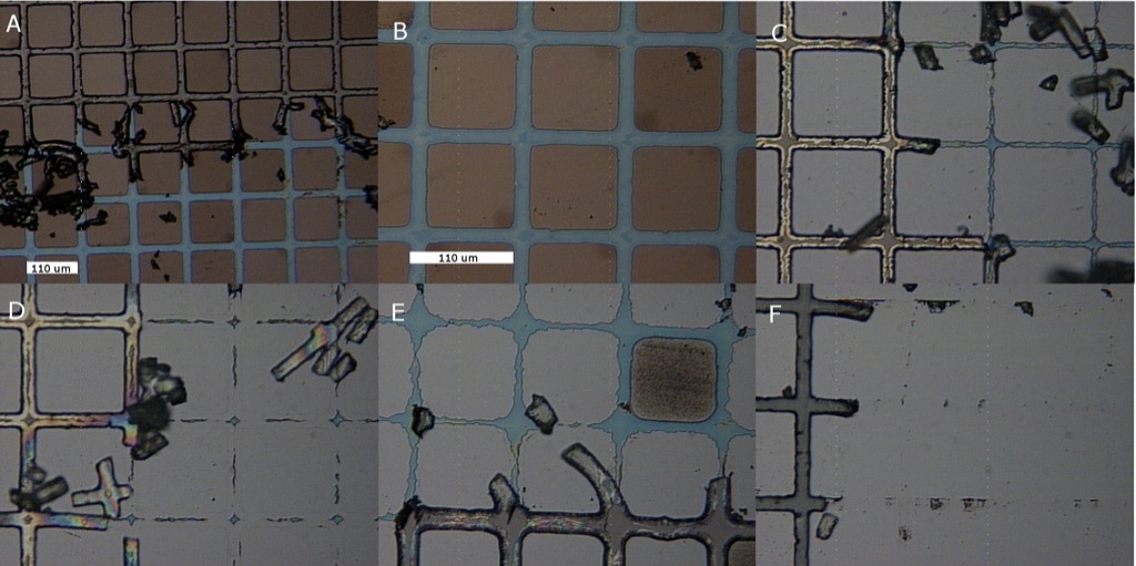
A) 150nm oxide with 10um lines after 1 min in BOE. SU8 has been scratched off the bottom portion of the image 10x mag. B) 150nm oxide with 10um lines after 1 min in BOE. SU8 has been scratched off, notice that there is still oxide in the open squares, indicating that in 60 seconds, 150 nm of oxide was not completely etched away?! It appears the SU8 structure slows the vertical etch, yet increases the lateral etching once the window is cleared. C) 150nm oxide with 10um lines after 5 min in BOE. SU8 has been scratched off the right portion of the image. D) 150nm oxide with 10um lines after 7.5 min in BOE. SU8 has been scratched off the right portion of the image. E) 150nm oxide with 10um lines after 8 min in BOE. SU8 has been scratched off the top portion of the image. This oxide is much thicker than the 7.5 minute sample. This is a good example of the surface not being clean before placing in BOE. The develop step is proving to be one of the most difficult steps in this process, often leaving a significant amount of residue on the surface. F) 150nm oxide with 10um lines after 10 min in BOE. SU8 has been scratched off the right portion of the image, no oxide remains.