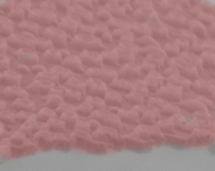
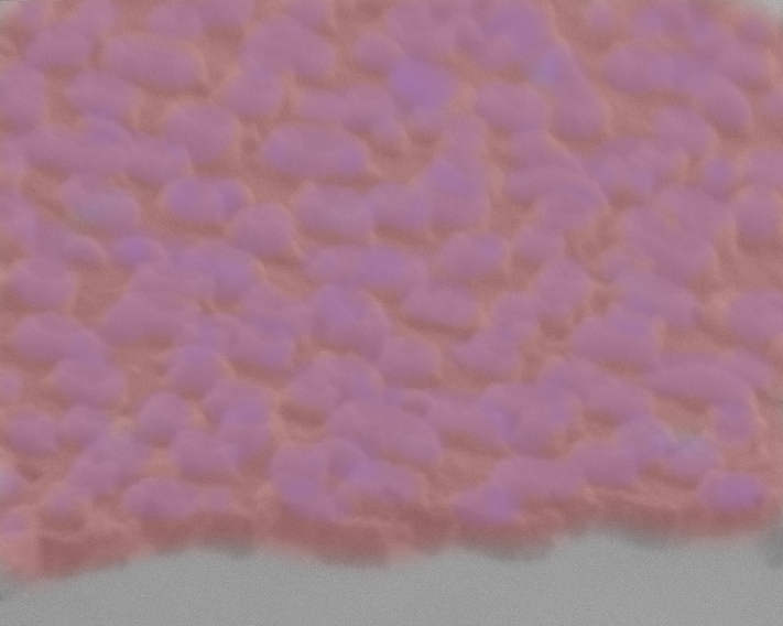
I have tinkered with the etch recipe some more, adding Argon to help prevent polymer formation (adding 5% O2 was not enough). The current recipe is 200 mTorr (100 mTorr Ar, 5 mTorr O2, 95 mTorr CHF3) at 120-125 W (6-12 W reflected). The plasma color is initially rosy (Argon), settling into a light purple after a few seconds (Light blue from CHF3 and O2 mix). After 140 seconds of etch using this recipe, the coated (250C, 1-3 A/s, 50nm) MgF2 films remain, while the backside is fragmented and discontinuous.
The true composition of these films has yet to be confirmed. Using EDAX on our SEM, I was able to find a decrease in the relative Silicon composition of the etched film, though some signal remains. I hope to get an XPS reading soon to confirm this result.
In the discontinuous film state, the etched free-standing membranes have survived for 48+ hours. The burst pressure for these films (SEPCON format) were 1.5 and 1 psi, much weaker than what we are used to having from nitride alone (thermal processing after deposition to densify the films may help in the future).
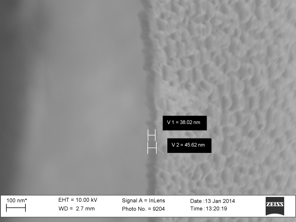
Step height on 50nm MgF2 film (kapton tape occludes deposition surface)
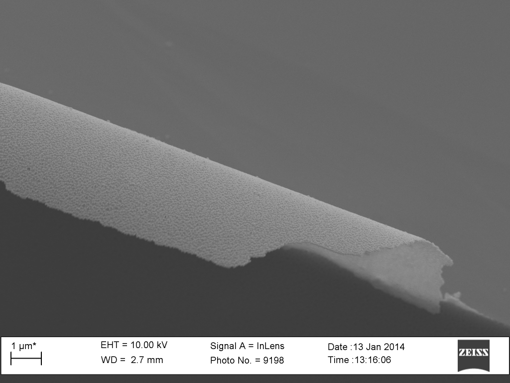
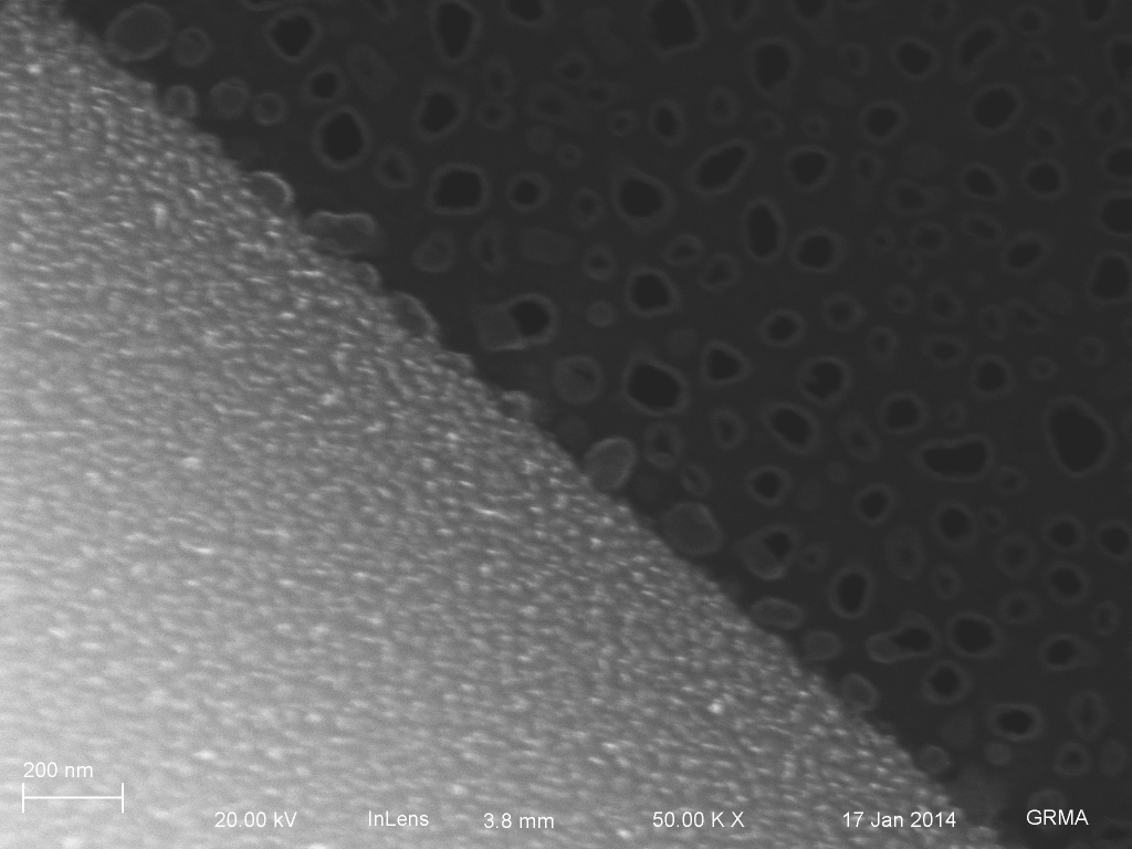
Sample 40, 50nm MgF2, 140s Ar+CHF3+O2 etch, curling up from freestanding region. The dark region is the bulk. The top face would be where the silicon nitride has been etched (backside)Sample 40, 50nm MgF2, 140s Ar+CHF3+O2 etch, curling up from freestanding region. The dark region is the bulk. The top face would be where the silicon nitride has been etched (backside). The film appears discontinuous, with little volcano structures remaining. Ideally, we would have none of these structures remaining with a more complete etch.Is the etched Film Pure MgF2?Or is the remaining film scummed up with Si3N4 volcano structures around the pore?
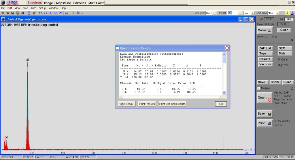
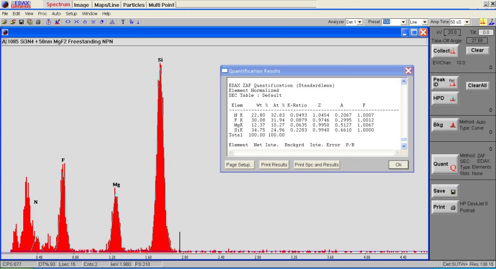
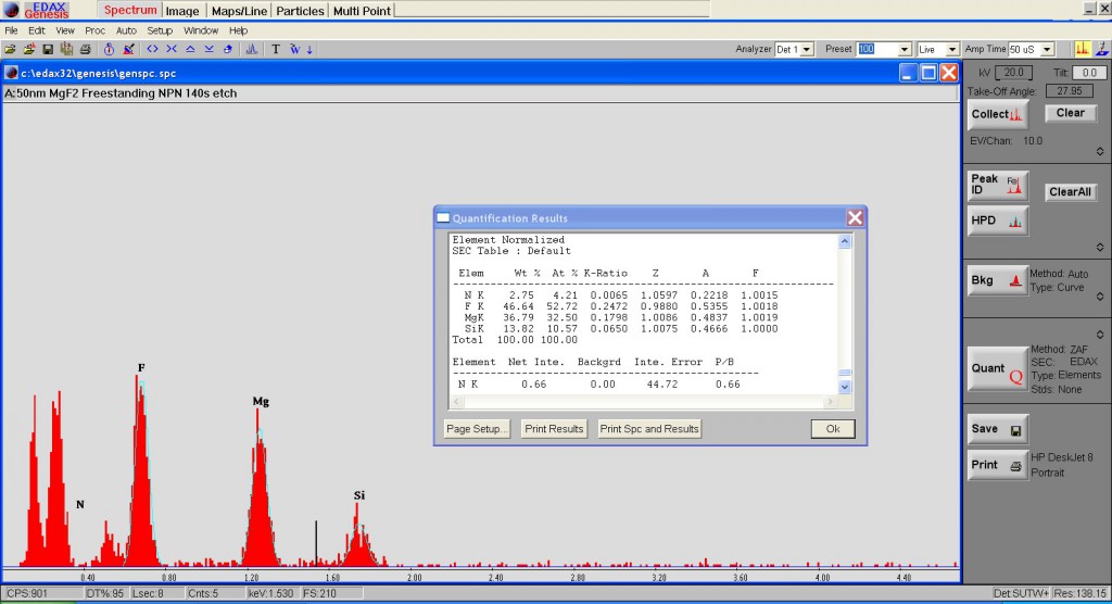
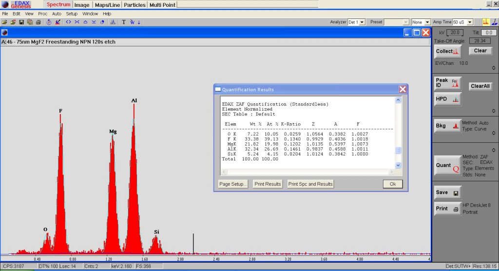
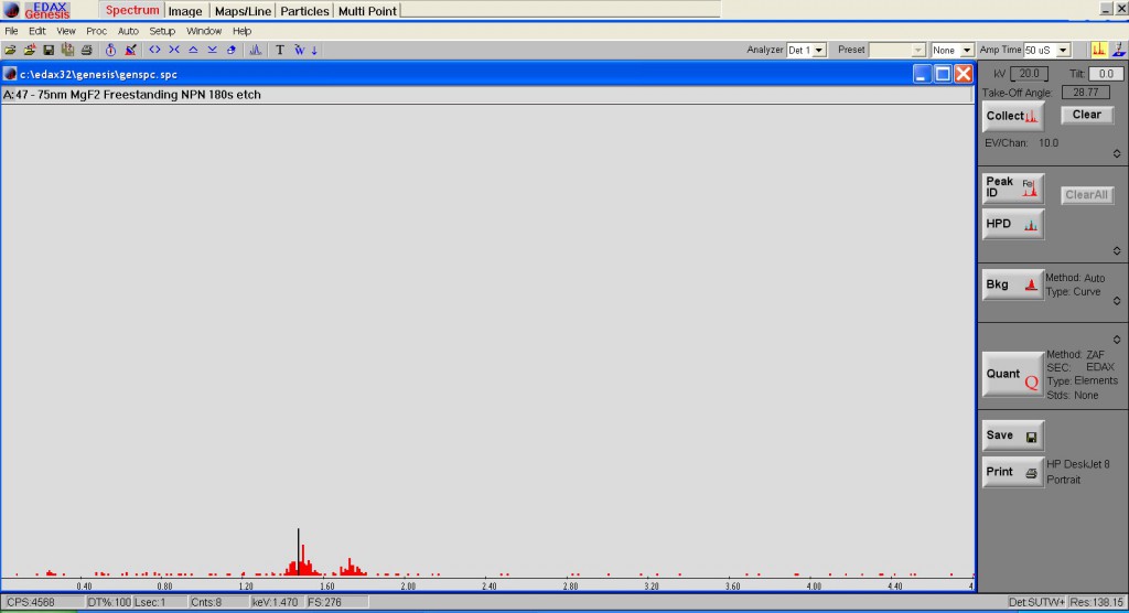
Control 50nm NPN EDAX measurement. Pure Si3N4 is expected.50nm NPN with 50nm of MgF2. This film has not been etched.140s Etched MgF2 membrane. Little silicon remains in the signal (85% MgF2). The larger peaks on the left are the Carbon background.I tried measuring another etched film with a different holder (Al). Again, the silicon signal remains. This sample had 120s etch (compared to 140s).This sample had 180s of etch, but no signal is coming out of the membrane? Clearly a freestanding region under SEM, and a measurement on the sidewalls of the chip confirm the EDAX detector’s functioning.
Sample 40, 50nm MgF2, 140s Ar+CHF3+O2 etch, curling up from freestanding region. Film thickness of MgF2 film is preserved.
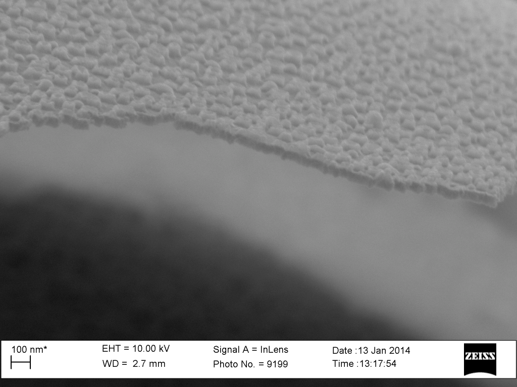
Sample 40, 50nm MgF2, 140s Ar+CHF3+O2 etch, curling up from freestanding region. Crossection shows the thickness of the MgF2 film remains the same.Sample 40, 50nm MgF2, 140s Ar+CHF3+O2 etch, curling down in freestanding region. MgF2 surface appears much smoother, with through pores apparent.
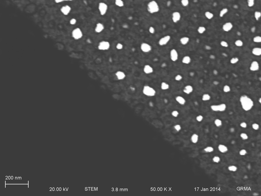
Sample 47, 180s etch SEM mode.Sample 47, 180s etch, TEM mode.
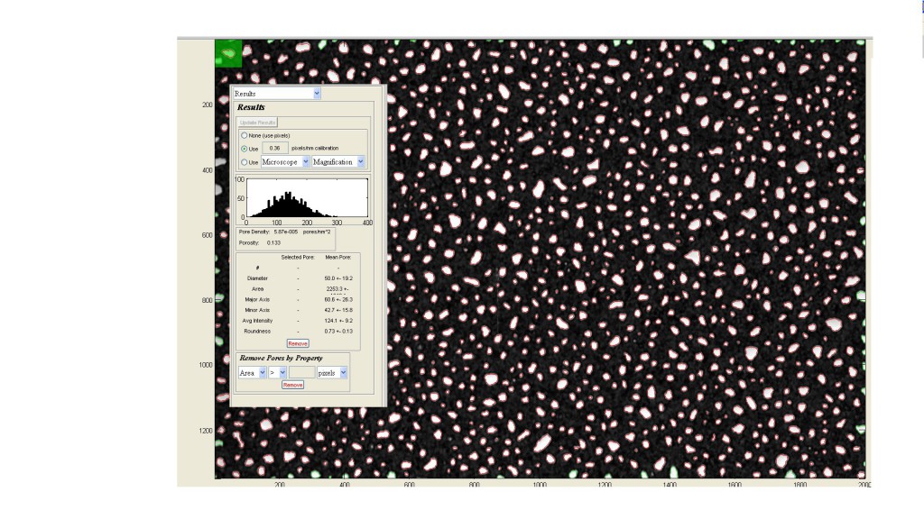
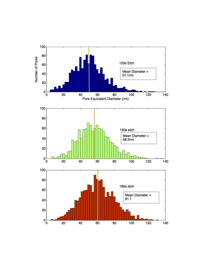
47 – Pore Histogram
Pore Histograms from samples 45, 46, and 47. Sample 45= 150s, 46=120s, 47=180s. Etching longer appears to blow out the pores somewhat, though the resistance is fairly high for 60s of additional etch time.
In my previous post, I derived a formula for the time-dependent flux decline in a centrifuge-driven membrane separation, assuming that the resistance of the membrane was held constant. The problem with that approach is that, as Josh discusses in this post, the resistance of the membrane increases with time according to one of several standard…
In this post we look at the effect of altering the area available for filtration on a standard 5 slot SepCon. Karl and I did this by simply cutting gaskets such that they covered different regions of the surface of a chip. We have three configurations, 1, 3 and 5 slots. Here’s a picture of…
Last week Jess helped me set up the diffusion cell with human albumin and cytochrome c. We ran 3 cells and used membranes from wafer 565. The membranes used were -1,4 (retentate 1), 3,3 (retentate 2), and 4,2 (retentate 3). The gel is posted below: The columns are (from left): Protein, control, retentate 1, filtrate…
As discussed in a previous post, we decided to test chips from wafer #1070 because they have smaller pores than those used in the most recent forward vs. reverse study. In the forward direction, 31 uL of filtrate was passed after 30 minutes at 3 krpm. (after 30 additional minutes at 5 krpm the total…
Summary of Results Membrane Pore Diameter Thickness Porosity Permeability (cc/cm^2*min*bar) SiN 3.2-4.0 um 0.12 um 22.1%-35.3% 30000 PCTE 2.4-3.0 um 9 um 11.9%-16.1% 1652 SiN Experimental Design Permeability of the 3 um pore Si Nitride membranes was assessed using the pictured apparatus: Fluid (ultrapure water) was pumped at a constant rate into a pipet whereupon…
Introduction This experiment is a continuation of previous work, cited below. Instead of urea spiked 1x PBS, whole heparinized bovine blood was pushed through the device over a period of four hours to then perform a urea assay on the separated and collected plasma. Please refer to the post below regarding the experimental setup that…