Frequency modeling of Ussing chamber (standard) and iBidi chamber
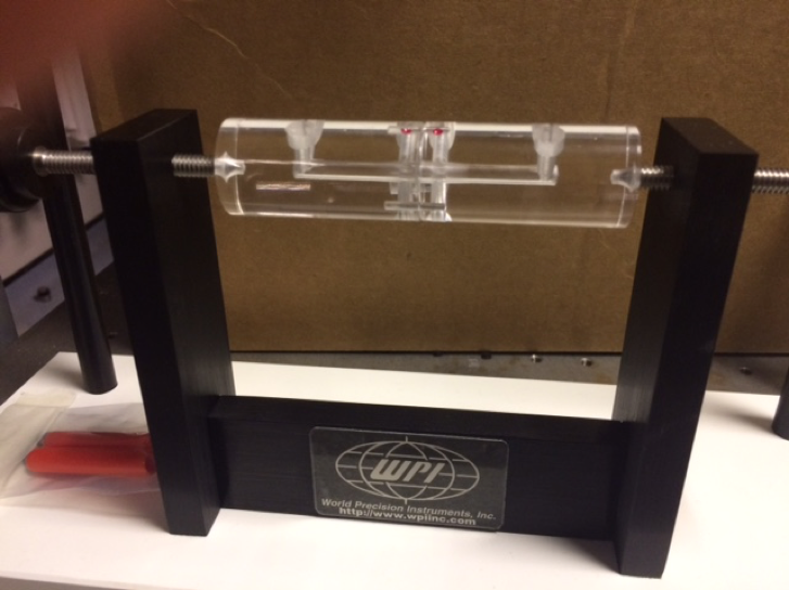
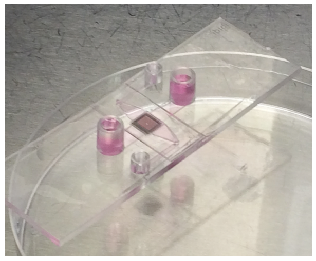
We desire to test the electrical perfomance of our membranes in the iBidi chamber. For comparison, I am using a gold standard Ussing chamber format to examine the contribution of our membranes to the overall frequency response of a system. I am using both a matlab model and a web-simulator (www.circuitlab.com) to examine an equivalent circuit model of these devices to see what kind of performance our setup will have. Different membrane formats, porosities, and materials as well as microfluidic access may limit what sorts of phenomena we can investigate in a particular device. Here, I take an example NPN chip and seal it into each of these devices. Eventually we will grow epithelial cells on these membranes in the devices and examine the properties of these cells by modeling out the known behaviors of the system.
Basically, the chips have very low capacitance and impedance, and shouldn’t affect our devices too much.
Ussing Chamber Modeling
Summary of parameters
- 1x PBS resistivity @ 25 C = 60-70 ohm-cm (http://web.mit.edu/dsadoway/www/118.pdf)
- 50 nm thick NPN chip, 40000 um^2 window (200×200 sq. um)
- Silicon Nitride relative permittivity = 8
- Conductance of a 30 nm diameter, 50 nm long cylindrical pore = 6.16e-8 mhos
- Pore density = 200 pores/ um^2
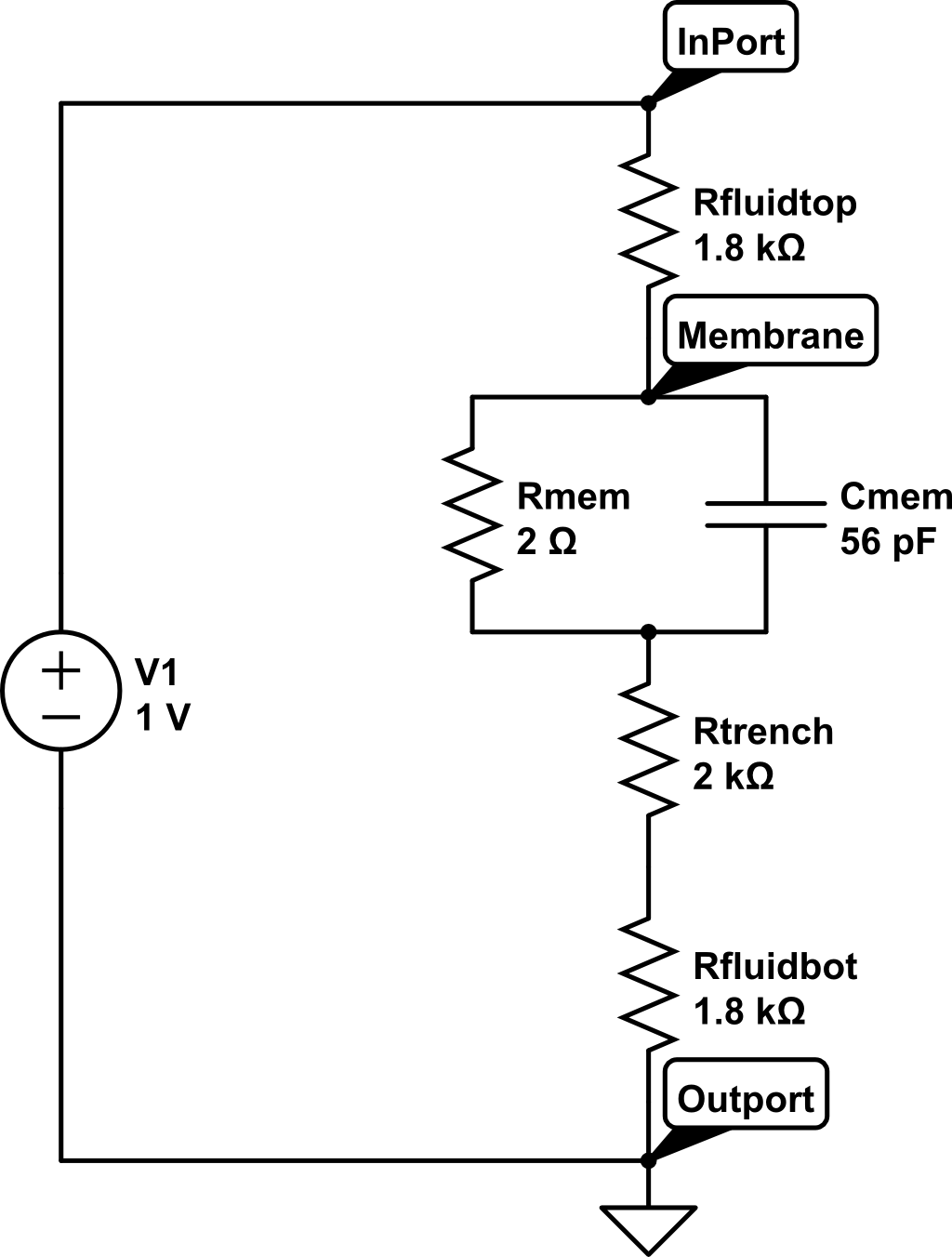
For the equivalent circuit model, I estimate the resistance and capacitance of the branches in the system.
The fluid branches are 4 mm diameter cylinders, total length 6 cm, which total about 3.6e3 ohms of resistance (1.8e3 ohms/branch).
The geometry (trench) of the chip introduces a constriction and to best estimate that resistance I used an estimated conical section of the trench of the chip (200 micron window opens up to a 6oo micron window). Reference can be found here, under section 6.4.4 (http://web.mit.edu/8.02t/www/materials/StudyGuide/guide06.pdf). This resistance is about 1.9e3 ohms = (72 ohm-cm)(.025 cm)/(pi*.01 cm*.03 cm).
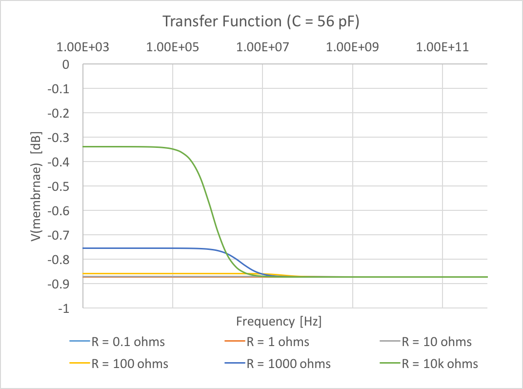
The capacitance of the NPN membrane I estimate to be less than 56 pF, because an unbroken, 50 nm thick, 200×200 um Si3N4 membrane has a capacitance of about (8*e0)(200e-6*200e-6 m)/(50e-9 m) = 56 pF, and a real NPN membrane has many tiny holes (~200 pores/um^2) in it.
The resistance of the NPN membrane I estimate to be around 2 ohms. For an average pore size of 30 nm, cylindrical pores, and pore spacing every 80 nm, the conductance of each pore is ((72 ohm-cm)*(5e-6 cm)/(pi*(1.5e-6 cm)^2))^-1 = 6.16e-8 mhos, and there are about 200 pores/um^2 (8 pores per .04 um^2) in my MgF2 images, so the total conductance of a 200×200 um membrane should be .4928 mhos = (6.16e-8 mhos)(200 #/um^2)(40e3 um^2), which is 2 ohms of resistance.
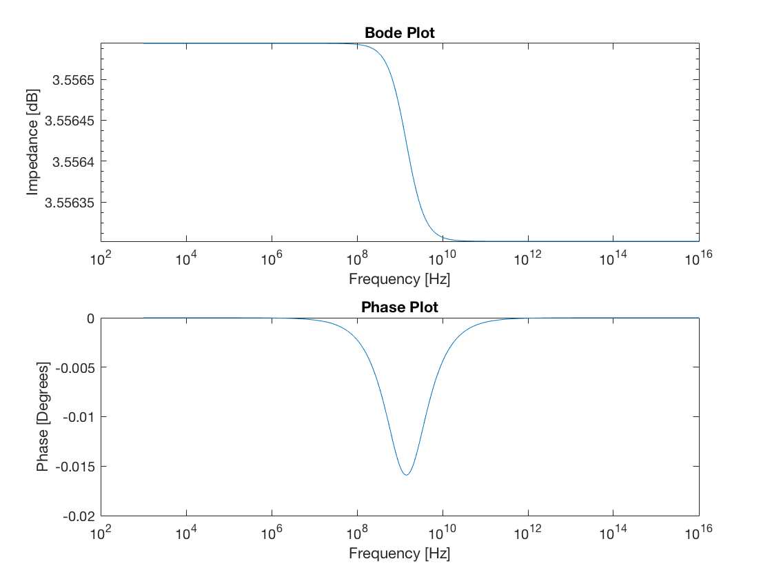
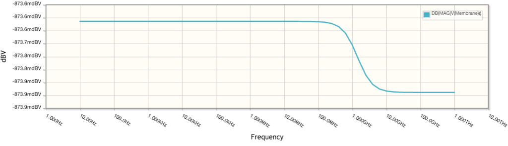
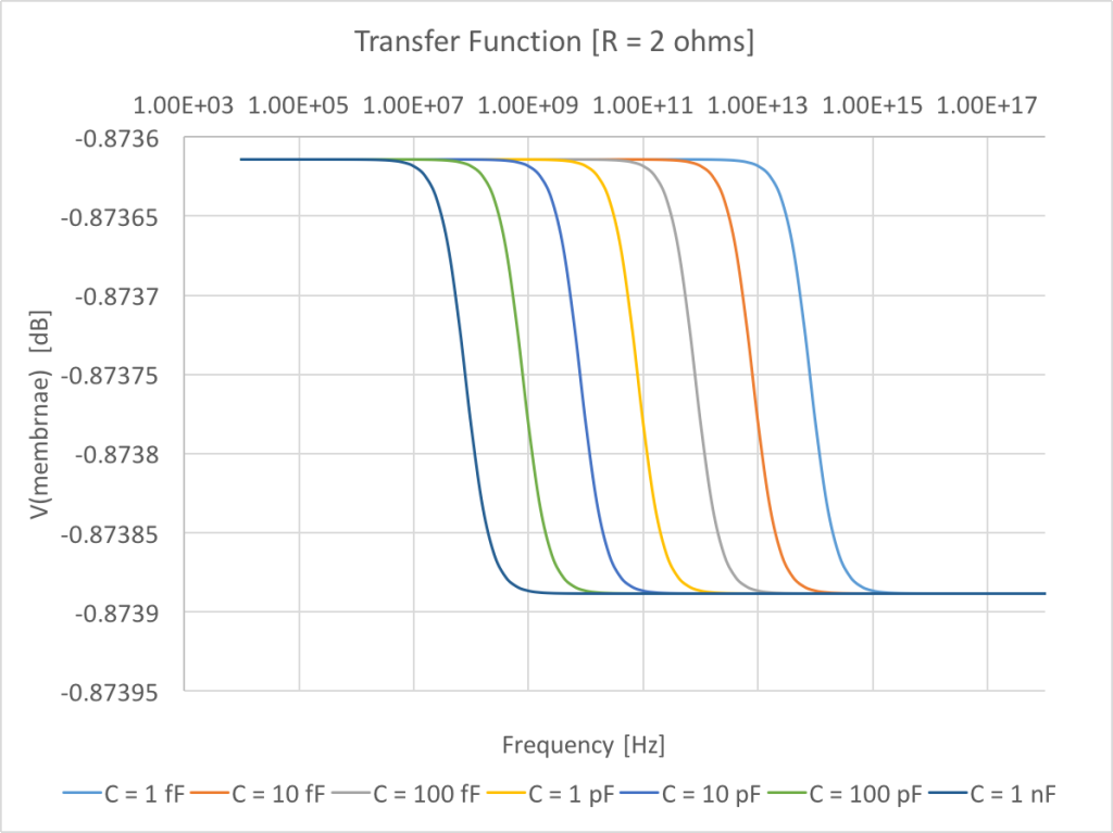
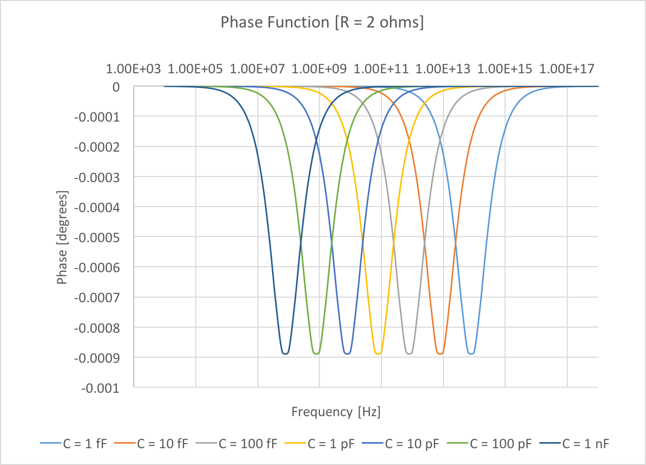
Transfer Function (voltage on membrane)
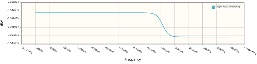
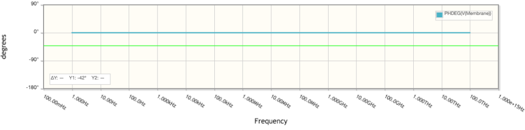
My Matlab code shows something similar, shown here calculating the overall impedance of the circuit (impedence_ussing – text file with m-code).
Resistance of Circuit
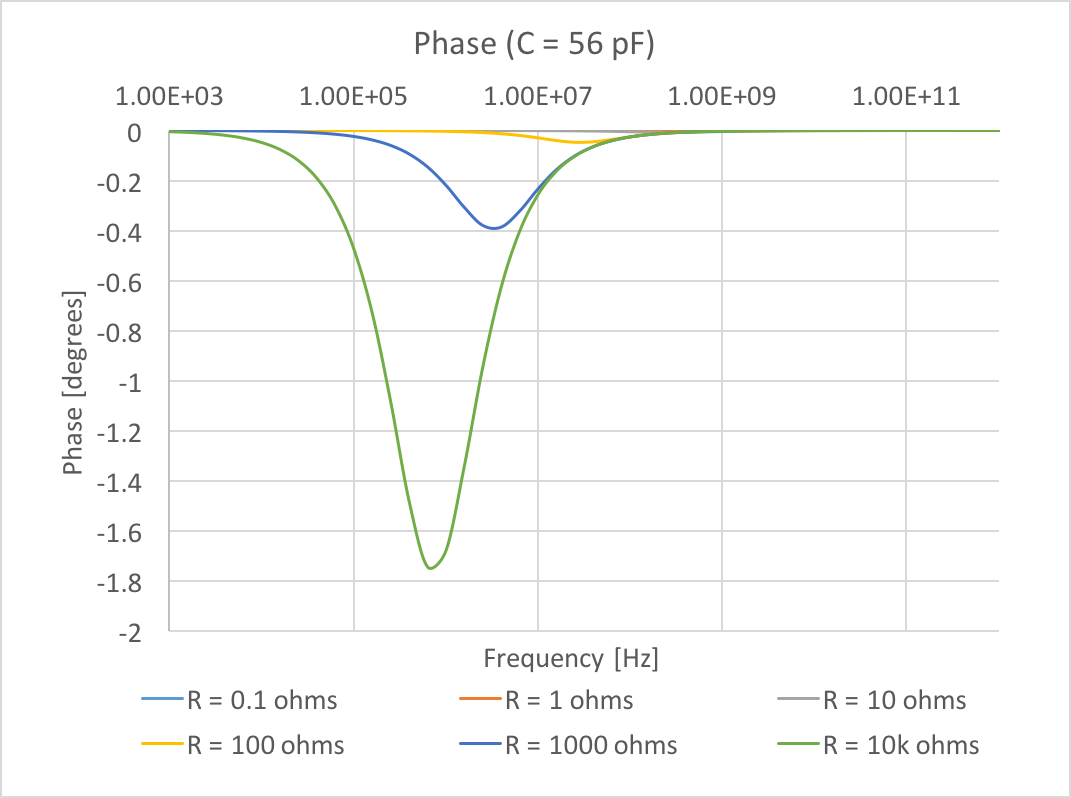
Family of curves (keeping all else the same in the above diagram)
Resistance of membrane (Rmem): As it increases, the overall proportion of the circuit’s resistance by the membrane increases, which means that as the capacitor forms a short circuit at high frequencies, it creates a larger change in resistance.
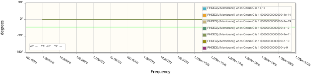
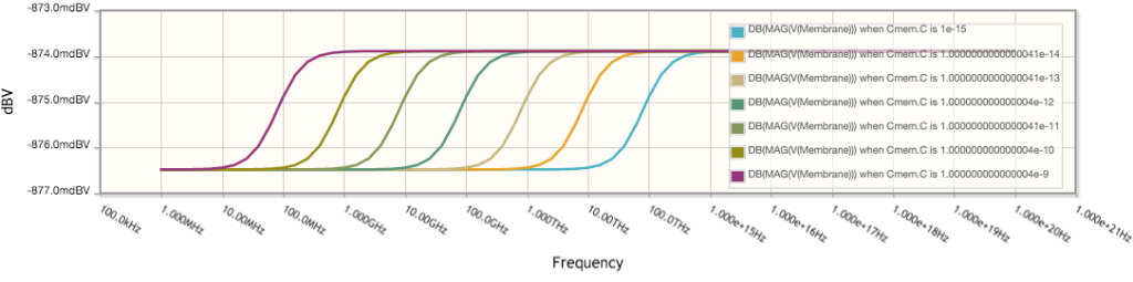
Capacitance of membrane (Cmem): Determines when the circuit will short out. Higher capacitances lower the pole frequency. Again, there is not much phase lag.
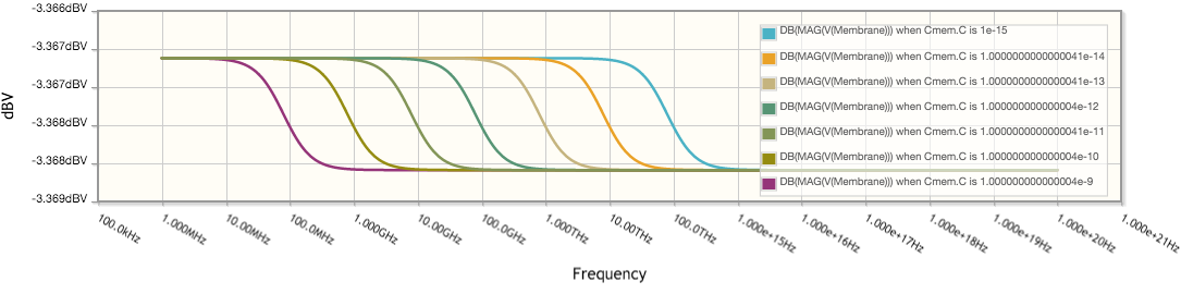
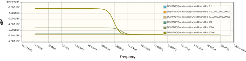
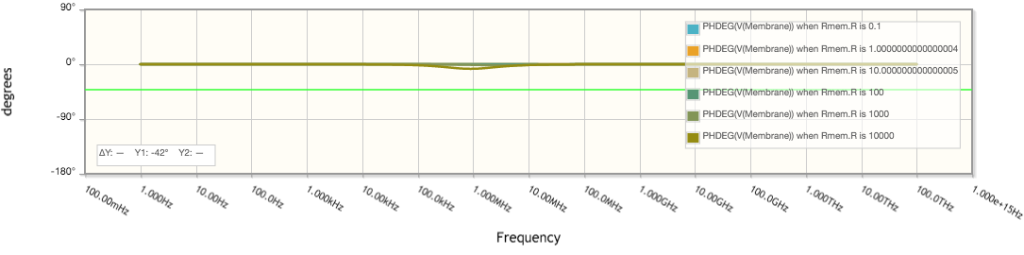
Ibidi Cell modeling
1x PBS resistivity = 60-70 ohm-cm
Bottom Channel (half) = 641 ohms = (70 ohm-cm)(1.1 cm)/(4x.02 cm)
Top Channel (half) = 4.156e3 ohms = (branch#1+branch#2+branch#3) = (2.33e3+1.6e3+116). *I’m using the worst case scenario for branch #2 [400, 1.6e3] (ie no diamond, only 1 mm wide)
R_mem = 2 ohms
C_mem = 56 pF

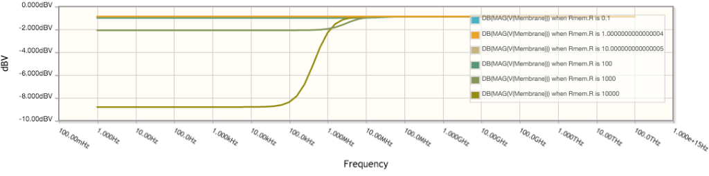
Transfer Function (voltage on membrane)

Circuit Resistance:

Family of Curves
Membrane Resistance (Rmem)
Membrane Capacitance (Cmem)
With this information, we should be able to make some basic measurements on our membranes.