Pore forming conditions
In the previous posts, I have shown that nanopores can be formed in silicon film sandwiched by two silicon nitride films. This discovery shows silicon nitride as an alternative barrier layer in the stack geometry. In this post, I’ll discuss a hypothesis about the pore forming conditions. The hypothesis is that either silicon dioxide or silicon nitride would not be the only barrier layer for the pore formation in silicon film. Nanopores can be formed in silicon film when sandwiched by other dielectric layers as long as they would not react with silicon film during the annealing. The true reason for the pore formation is the defect nature of the sputtered silicon film and the rearrangement of silicon atom during crystallization. This hypothesis needs to be further proved. Since the alumina is also a dielectric film, the experiment that I have done in the last week was annealing of free-standing nitride/silicon/alumina (NSA) and oxide/silicon/alumina (OSA) stacks.
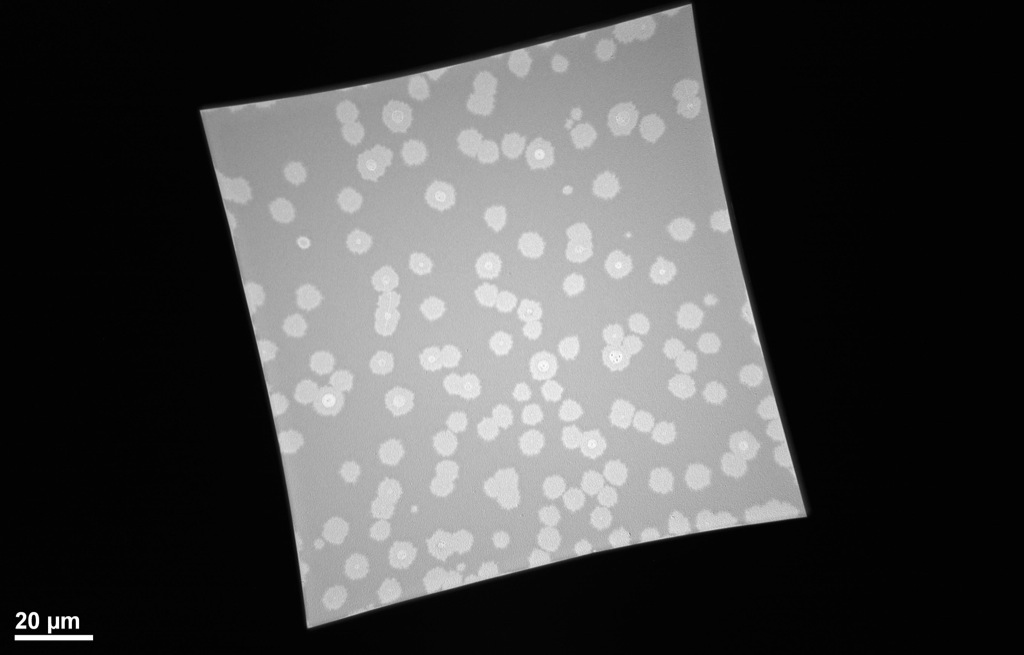
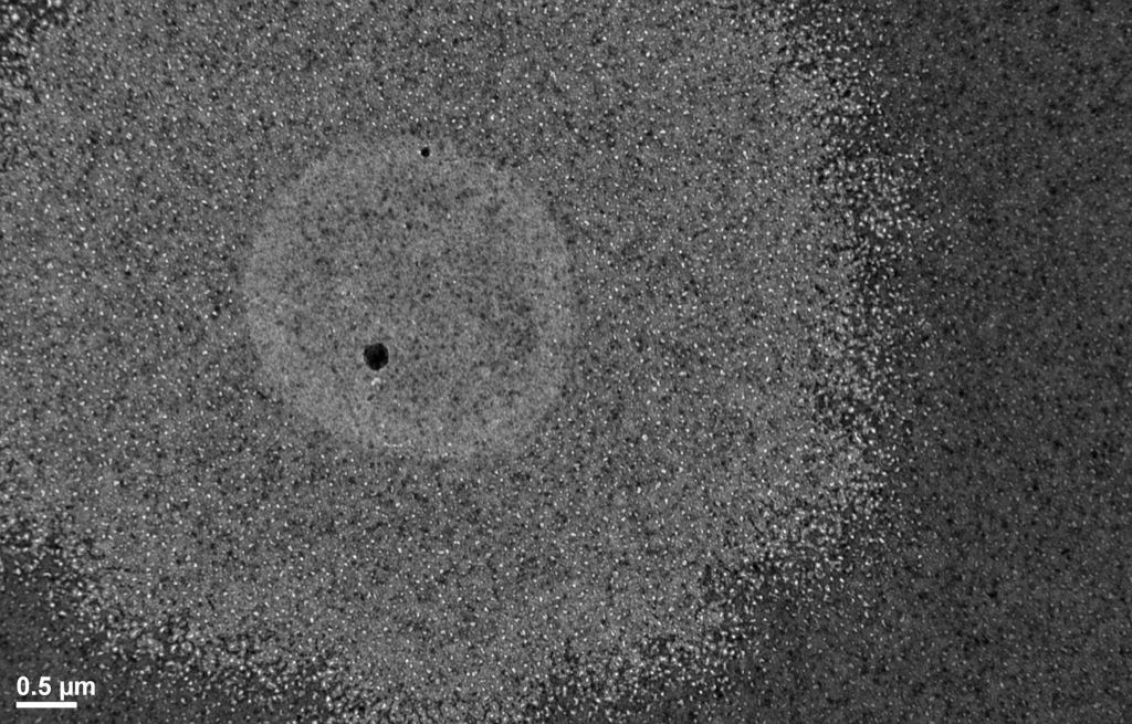
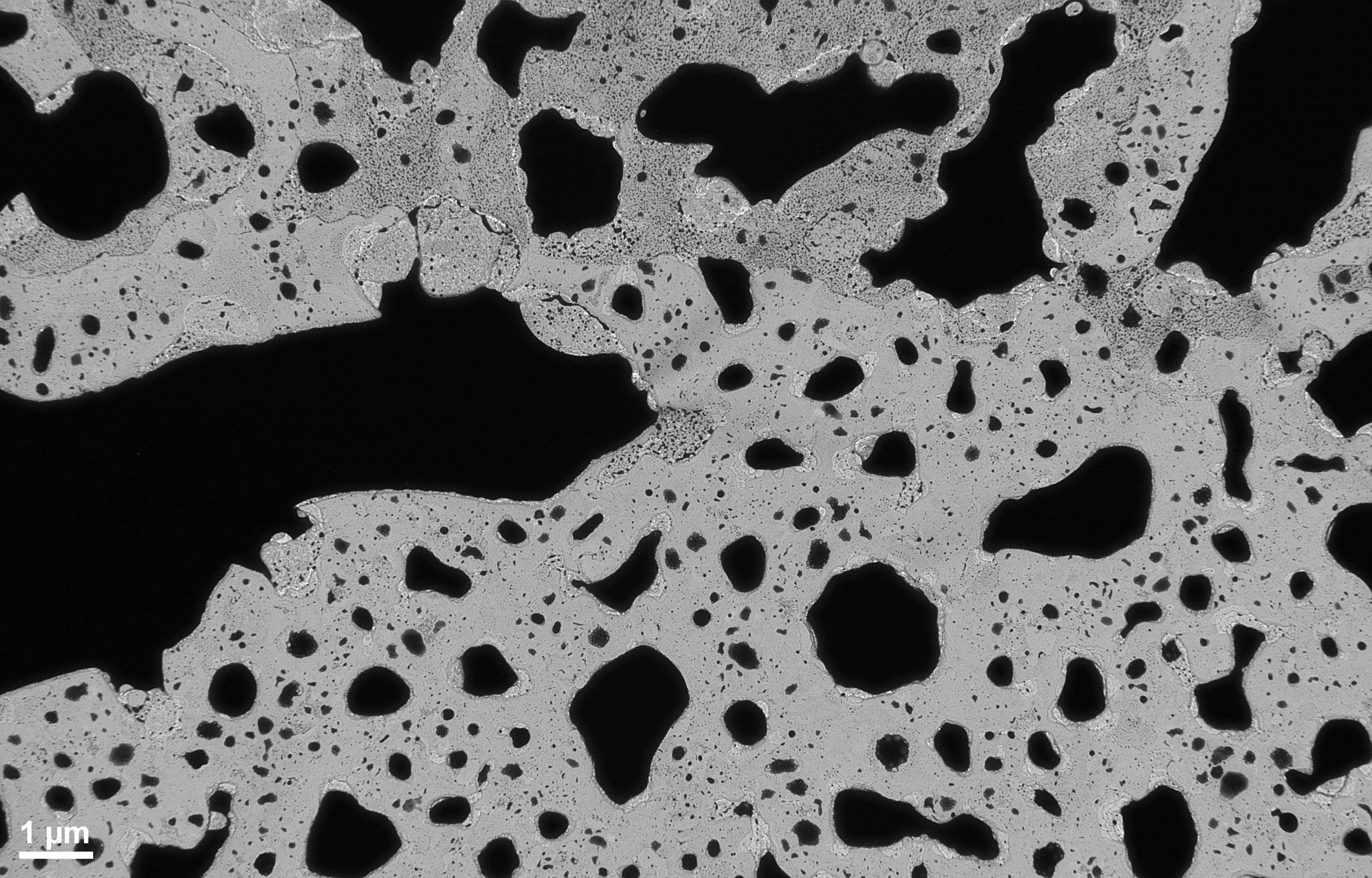
Aluminum oxide film was deposited onto the free-standing silicon nitride/amorphous silicon and silicon dioxide/amorphous silicon membranes using ALD. The thickness for the silicon film was 15nm while the nitride, oxide and the alumina were both 20nm thick. After deposition, the free-standing NSA and OSA stacks were RTP annealed at 1000C for 1 minute with a 50C/s ramp up rate. The followings are the TEM images of annealed NSA and OSA stacks.

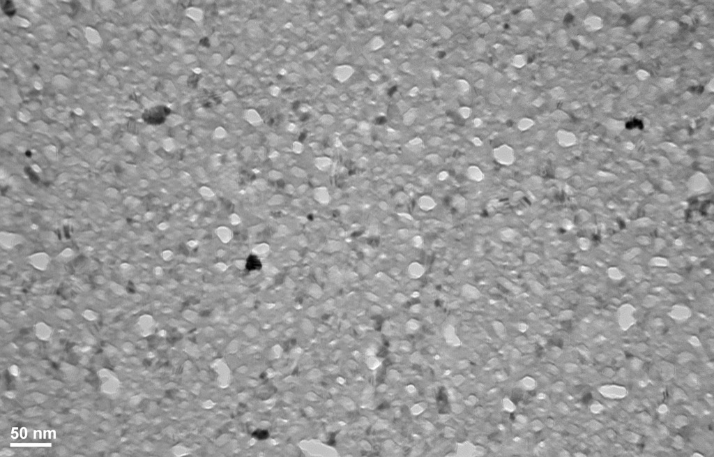
From the TEM images it can be clear seen that nanopores are formed in the silicon film. The pore size and porosity are relative small compared with nanopores from the NSN stack.
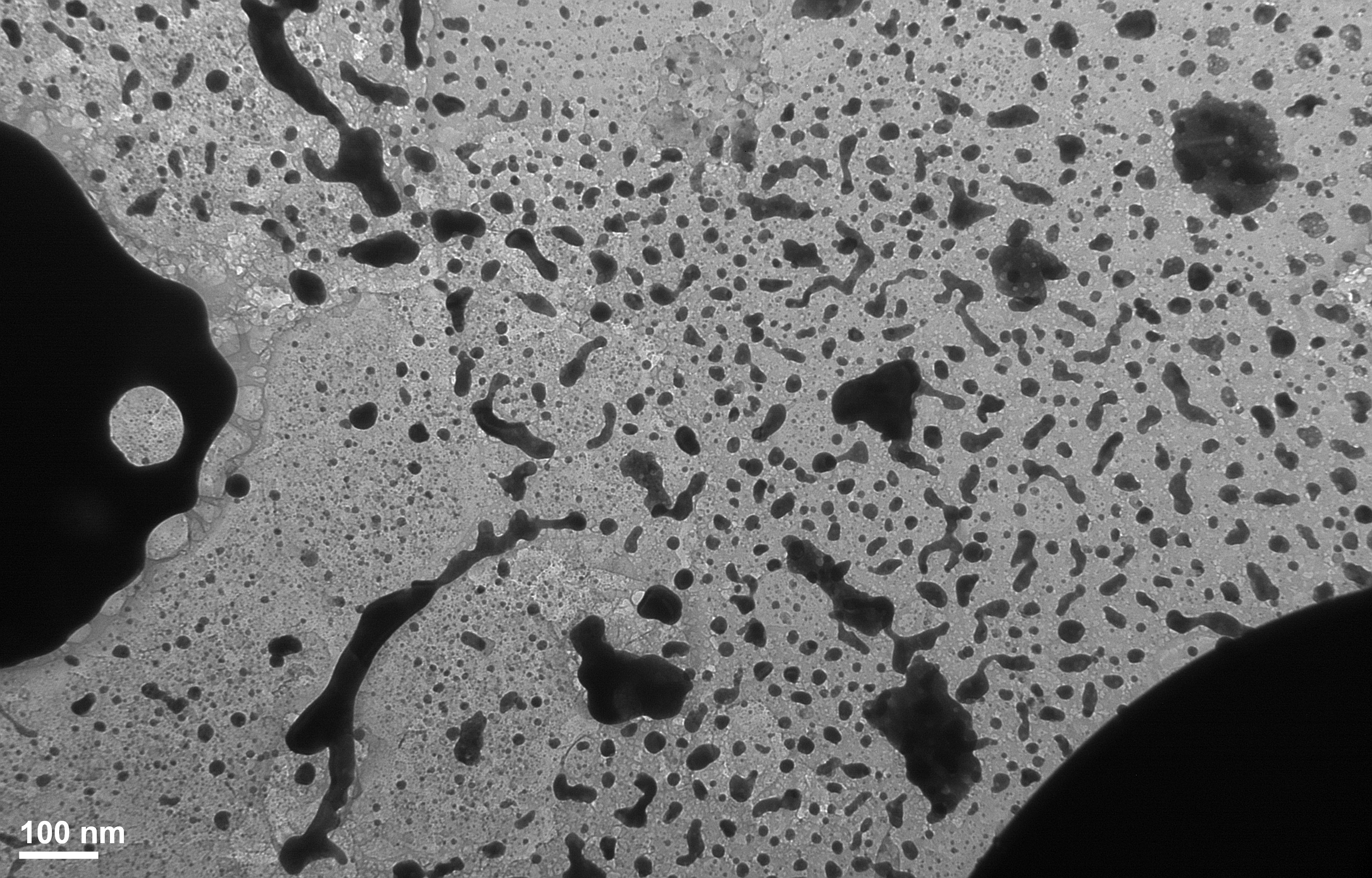
Next are TEM images from annealed OSA stacks. One thing needs to be mentioned here is that the alumina was not able to fully removed in the HF solution.
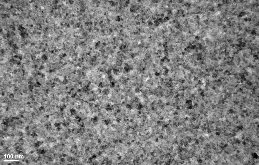
It seems that nanopores are also formed in the silicon film from the OSA stack. However, because of the residue alumina on top of the silicon film, it is relative hard to see the open pores from the TEM images. I’ll try to use the HCl acid to remove the alumina first and then strip the oxide using the HF next time.
In contrast to alumina, I also deposited a metal film-20nm thick Platinum on free-standing NS and OS membranes. The following TEM images are annealed NSP and OSP membranes (same annealing condition as above).
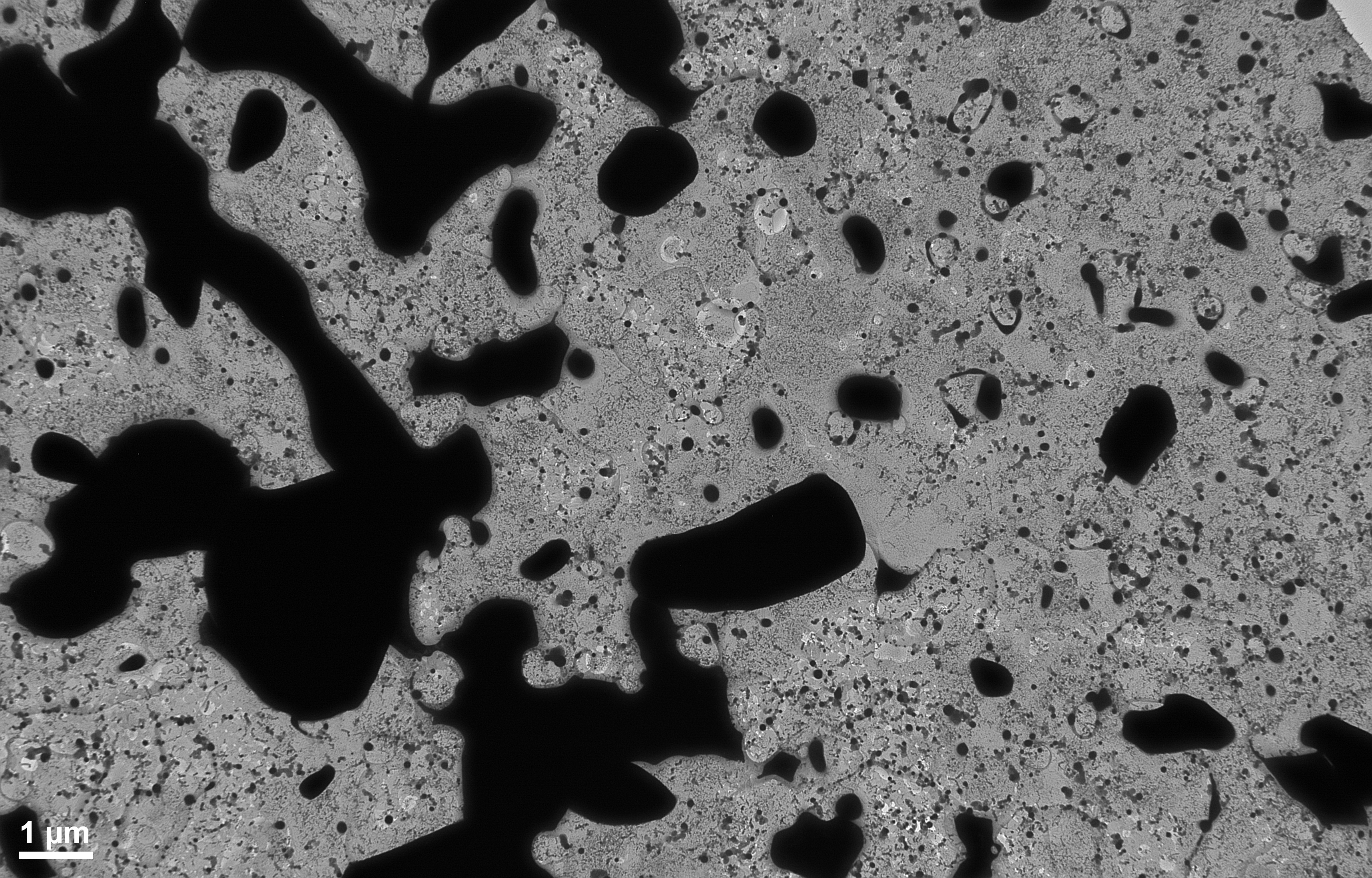
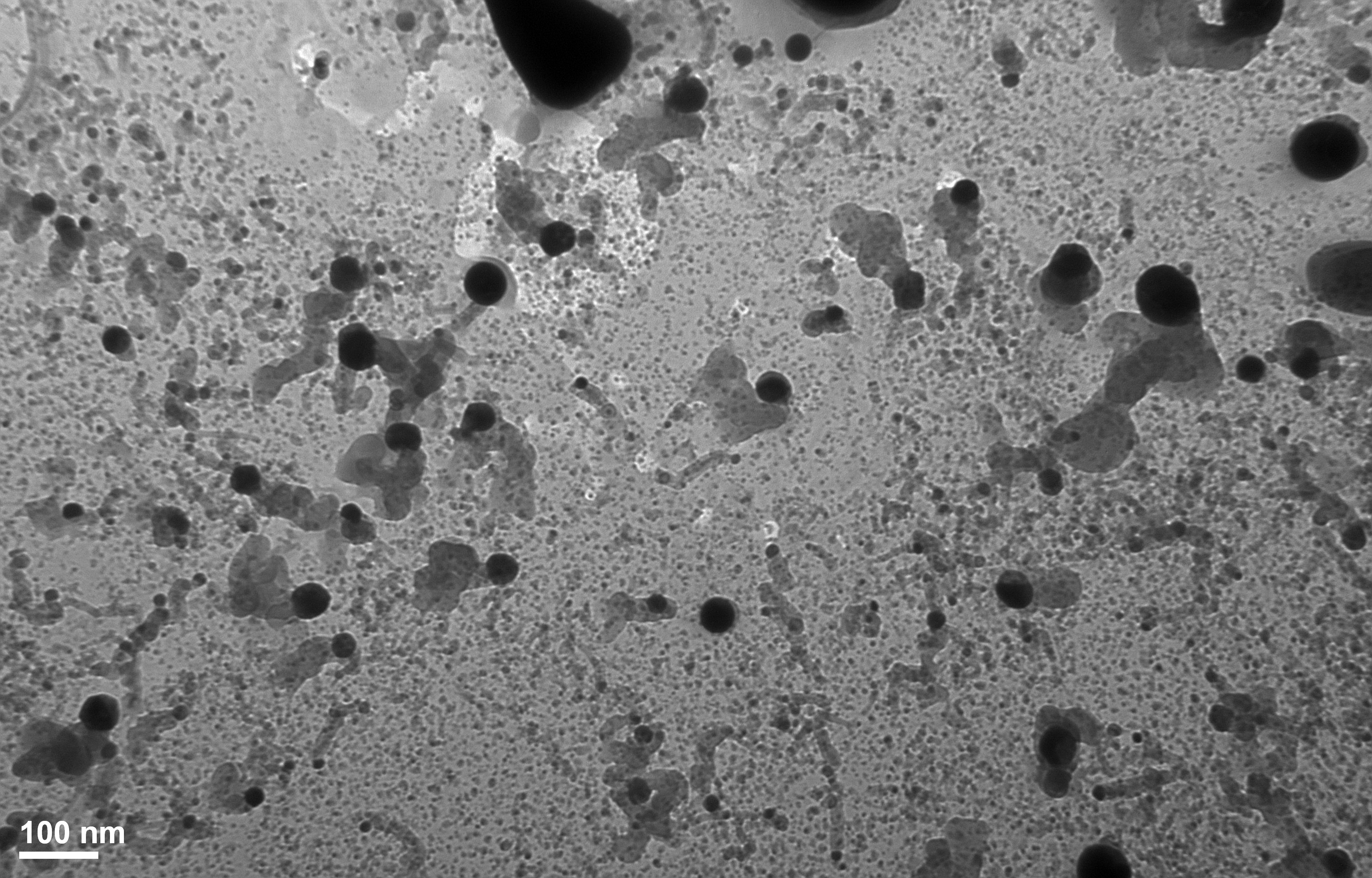
From the above TEM images, it can be seen that the platinum film agglomerated during the annealing process in both NSP and OSP stacks. It is hard to tell whether nanopores are formed in the silicon film from the TEM images.
In sum, it has been shown that nanopores can be formed in the silicon film with different barrier layers including oxide, nitride and alumina. It indicates that the nanopore formation phenomenon is relatively dominated by the property of sputtered silicon film while the barrier layers also affect the pore formation process and pore characteristics.