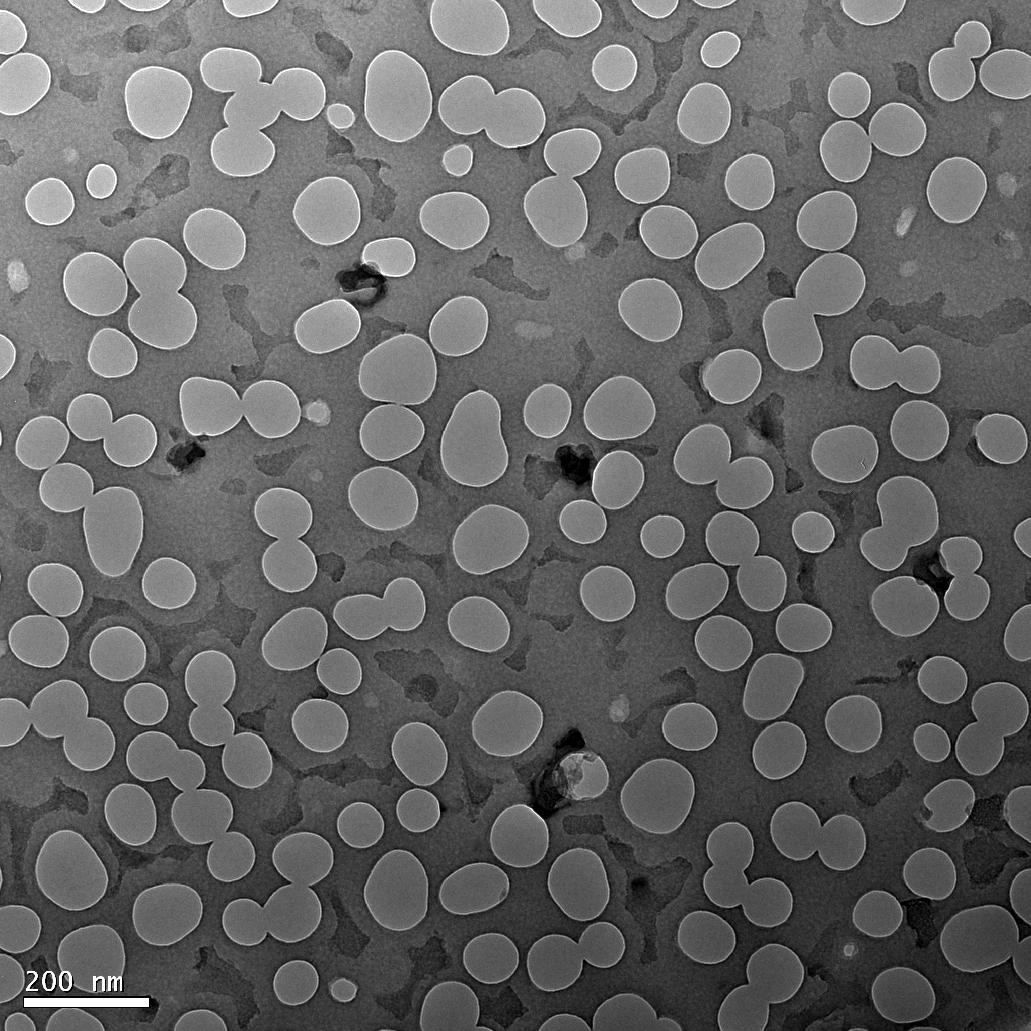
1255 (100nm NPSN) Partially Etched Super Thin TEMs
I’ve been trying to recover a pore distribution from my 1085 MgF2 SERS wafer that had a ~60 nm pore size on average. This has been difficult with thinner, 50 nm NPN because there is less material to shape; it’s harder to stop at a certain point to get the right pore distribution. So, using a thicker material should allow some more process flexibility to arrive at the correct distribution. I’m using some of the 100 nm 1255 NPSN material to test out to what degree I can etch and achieve the correct distribution. 1255 has one large rectangular window.
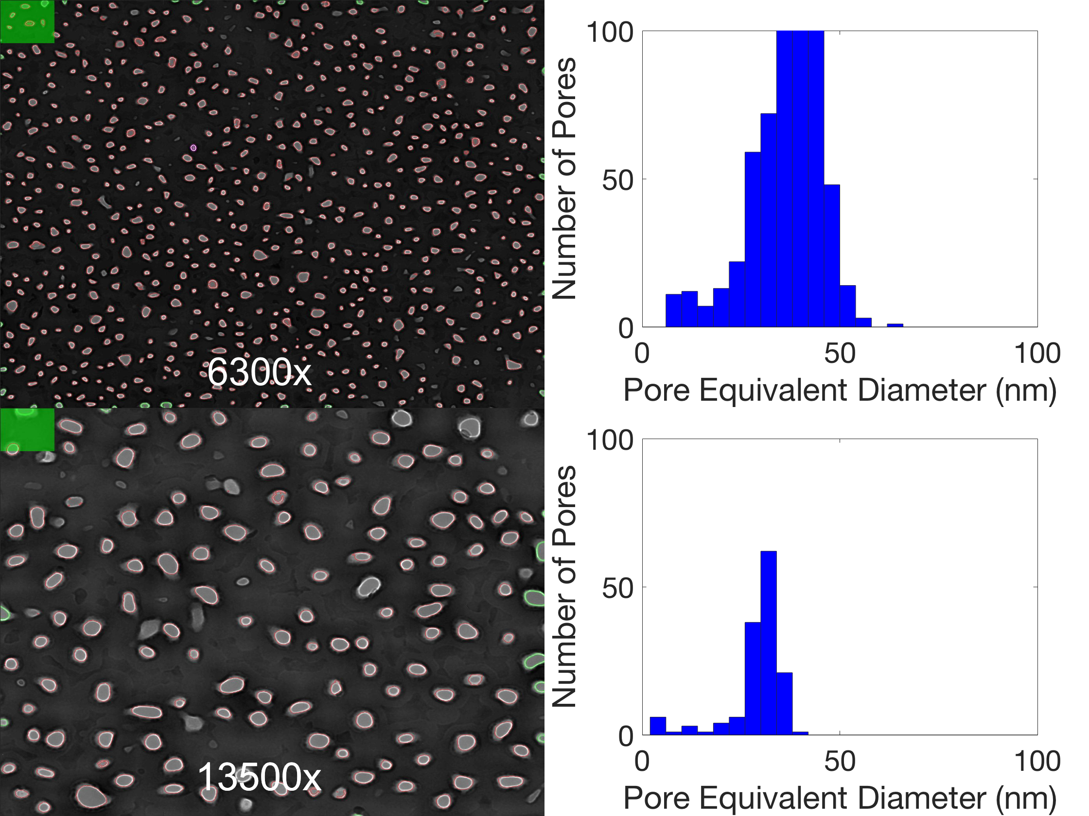
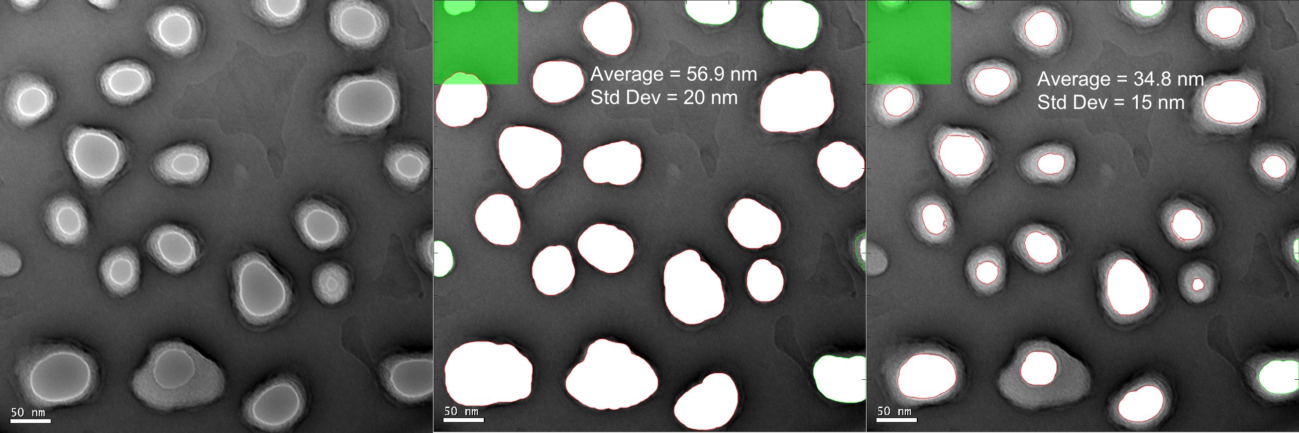
I used a SF6/CHF3 etch as described in this post to remove material from the backside of the nanomembrane (etched the trench). This preserves the front surface more (etch will still attack sidewalls) and allows for a more fair comparison. However, it seems that I overetched considerably.