Changes in nanocrystalline structure due to mechanical stress
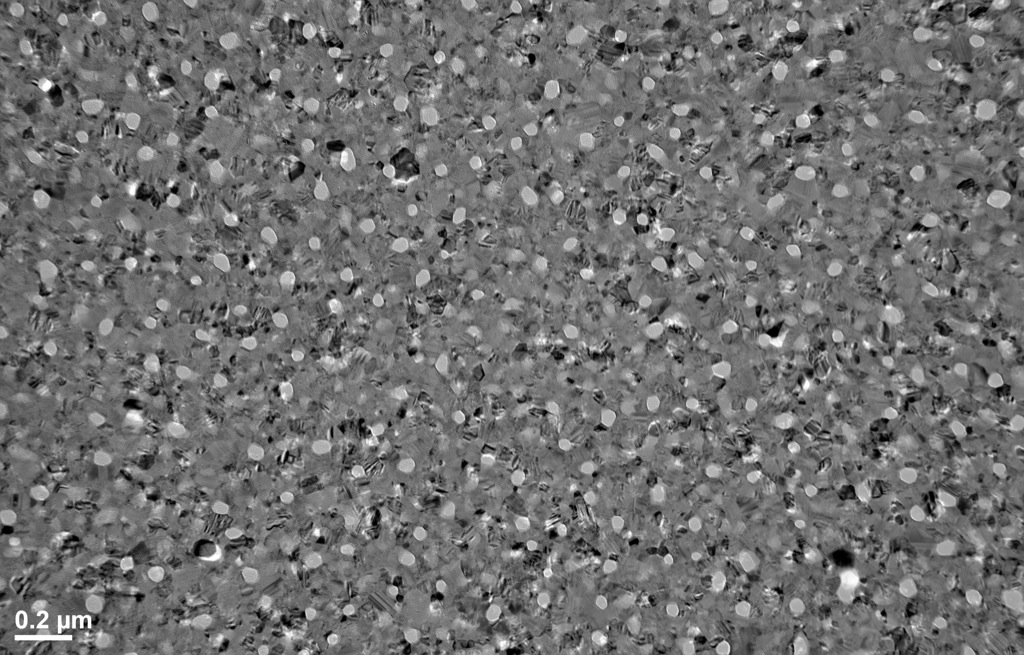
One of the things that I’ve been working on recently is trying to explain the extreme elasticity of the pnc-Si material which is connected to its nanocrystalline structure. There are two parts in this question. First, how are amorphous or crystalline phases involved during stretching? Second, does the crystalline phase change under application of mechanical stress and how? The stretching is very hard to observe as it requires in situ TEM tensile stressing. I tried looking at the SEM images of the stretched membrane which was hardened bulged by cured polymer behind it. I hoped to see the changes in distance between pores, but it is too small to be noticed. The images look very similar.
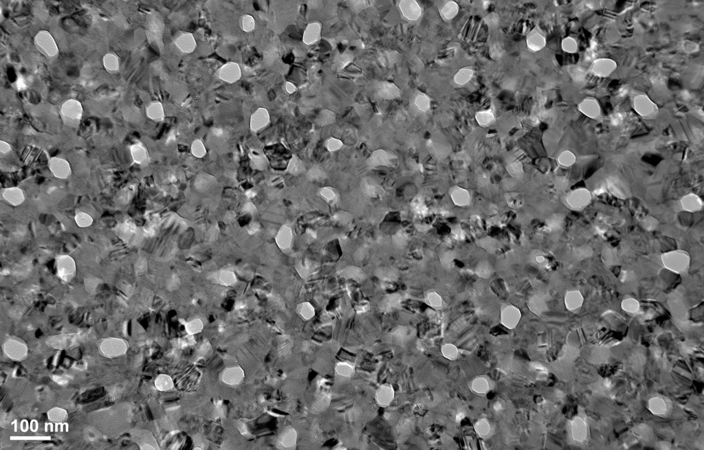
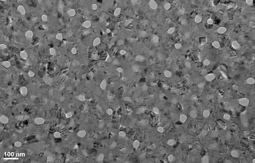
Now, in terms of the mechanical stressing: The following experiments are the first successful TEM images of the same area of the membrane before and after the mechanical stressing. To find the exact same spot, Dave and I spend most of the time trying to put together coordinates form two different corner measurements and chasing the same pore patterns which are perfect marks in this kind of work.
The shown area is approximately 20-30 micron away from the middle of the edge towards the center of a square membrane, where the highest stress is expected. The stressing is done in the pressure cell by pressurizing the TEM samples to up to 3 psi for 1 minute few times.
I didn’t have time yet to analyze the images but the first impression is that nothing happens to most of the bigger crystals, and this is probably due to them having open surface on both sides of the material. Some of the smaller crystals probably rotate and become not visible. Also looks like some of the twin crystals change. Crystal rotation and “re-growth” of twins are common in other nanocrystalline materials that’s why I think it could be the case.
TEM 50k before and after

Before and after 100k
I’m impressed that you were able to come back to the exact same spot. That’s quite impressive, and I can think of some interesting annealing experiments that could be done to try and observe crystal coalescence or instability in the pores.
However, I’m not convinced that the material has changed, rather the illumination angle or something about the imaging conditions appears to be different. IF you look at some of the diffraction artifacts from the larger, “stable” crystals, something is very different. I think you need to run a side-by-side control that was not pressurized, to normalize out such imaging differences. You would not need to pick a high-stress point, so could use an area near a corner that would be easier to find. Still, the images look very different, and it would be useful to figure out why. If these were from 2 different fabrication runs, I would definitely interpret the crystalline fraction and nanocrystal size differently.
Dave – do you think the material actually changed, or do you think the imaging conditions (integration time, focus, angle, contrast mode, stigmatism, beam size, voltage, current, etc.) could be different?