pnc-Si membrane from silicon nitride and silicon oxide system
Now we already confirmed that pores are able to form in both oxide/silicon/oxide and nitride/silicon/nitride system. Here comes an interesting question- how about nitride/silicon/oxide and oxide/silicon/nitride system? In the past week, another two different stacks including SiN(30nm)/ a-Si(25nm)/SiO2(30nm) and SiO2(30nm)/a-Si(25nm)/SiN(30nm) were tested. The nitride film was deposited with 25 W bias and the silicon with 5W bias. The silicon dioxide was deposited without bias.
The followings are the TEM images of SiN/a-Si/SiO2 free standing membranes with removing the substrate first annealed at different temperature. The annealing time and ramp rate are 1 minute and 50C/s for all samples. The annealing temperature from (a) to (f) are 800C, 900C, 1000C, 1050C, 1100C, and 1150C, respectively.
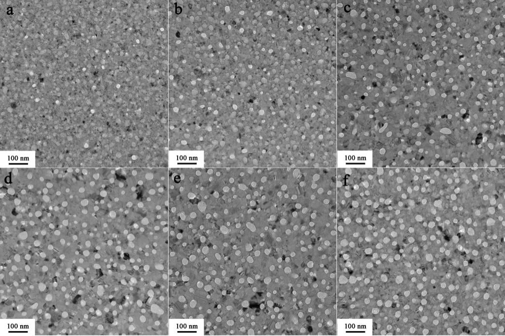
It can be seen that more and bigger pore are opened up with the increasing anneal temperature. The porosity and pore diameter plot clearly proves the trend of pore evolution with annealing temperature. The porosity increases rapidly from 0.8% at 800C to 13.3% at 1050C and it finally reaches to 16.3% at 1150C. The diameter increases pretty linearly with the annealing temperature. From the pore distribution plot we can also see that the distribution curve becomes broader with the annealing temperature, which indicates that the pores grow bigger and bigger.
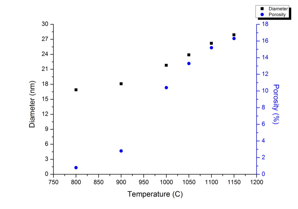
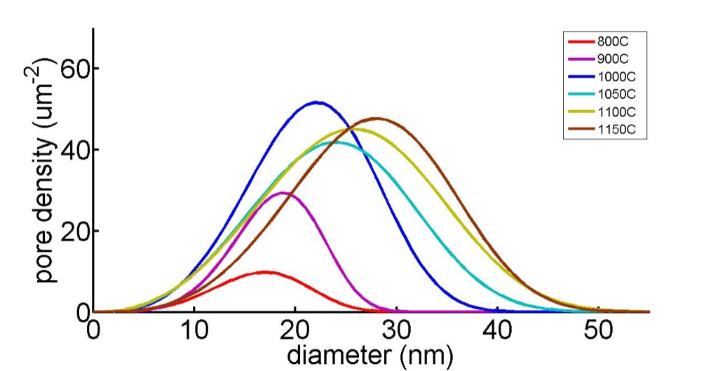
This result shows that the SiN/Si/SiO2 stack behaves quite similar to SiN/Si/SiN stack in terms of the pore evolution with annealing temperature. The only difference is that the later stack yields higher porosity and slight bigger pores.
The SiO2/Si/SiN stack, however, shows quite different behavior than the other two stacks. Same annealing conditions were tested on the SiO2/Si/SiN free standing stack and the followings are the TEM images. From the TEM images it can be seen that very few pores are opened up when the annealing temperature is below 1000C. It can be also seen that the sizes of silicon crystals increase with the annealing temperature.
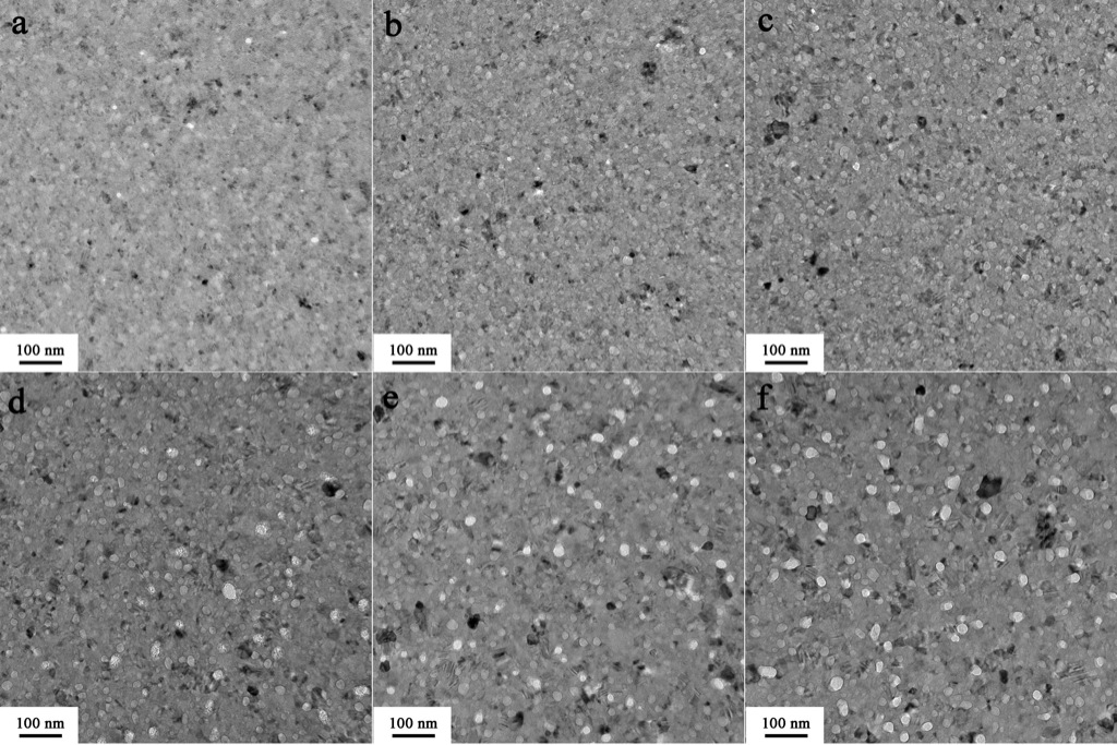
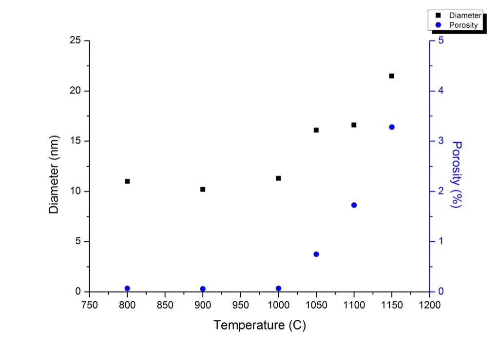
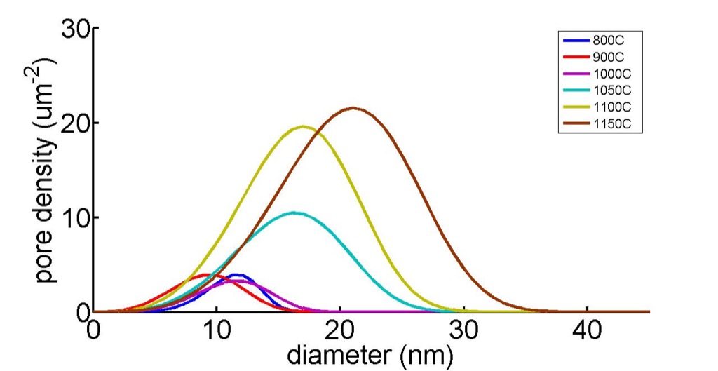
From the porosity plot, it can be seen that the porosity almost does not change and keeps very small around 0 when the annealing temperature is equal or less than 1000C. Very few small pores around 10nm are formed at this condition. When the annealing temperature is greater than 1000C, more pores start to opened up and the porosity as well as the pore size start to increase. The porosity reaches to 3.2% when annealed at 1150C, which yields around 21nm pores in average diameter. The pore distribution plot also shows the similar trend.
Compared the SiO2/Si/SiN system with the rest two (SiN/Si/SiN and SiN/Si/SiO2), it can be seen that the pore evolution is quite different when the annealing temperature is below 1000C. Very few pores are formed in SiO2/Si/SiN system and both the the porosity and pore size almost do not change when the SiO2/Si/SiN membrane is annealed from 800C to 1000C where the porosity and pore size increases rapidly with the annealing temperature for SiN/Si/SiN and SiN/Si/SiO2 membranes. It may be because that the SiO2 film is less stressful since it was deposited without bias and the intrinsic stress is more likely the key factor to drive the pore formation. It also indicates that the lower interface is more important to the pore formation.
Next I’m gonna deposit thinner silicon film in nitride/silicon/nitride stack, biased oxide film in oxide/silicon/nitride stack and oxide/silicon/oxide control sample.