High porosity pnc-Si membrane from nitride/silicon/nitride stack
Last week, I deposited silicon nitride/ amorphous silicon/ silicon nitride stack and then annealed the free standing stack after etching the substrate. The nitride film was deposited with 25W bias and the silicon film with 5W bias. The thickness for the nitride film is 30nm where it is 25nm for silicon. One of the initial purposes to switch to nitride stack is to verify whether the thermal stress due to the differences in thermal expansion coefficients is the driving force to form pores during annealing. The reason is because the thermal expansion coefficients of amorphous silicon (2.6×10⁻⁶/K) and silicon nitride (3.3×10⁻⁶/K) are very close, where silicon dioxide has a quite low thermal expansion coefficient which is only 0.4×10⁻⁶/K. The result turns to be very interesting because high porosity pnc-Si membrane in the nitride stack was observed. The followings are the TEM images of SiN/a-Si/SiN free standing membrane annealed at different temperature. The annealing time and ramp rate are 1 minute and 50C/s for all samples.
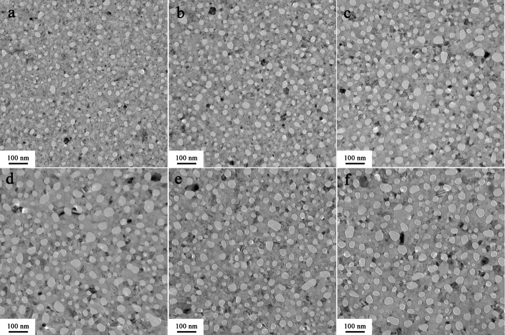
The annealing temperatures from image (a) to (f) are 800C, 900C, 1000C, 1050C, 1100C and 1150C respectively. From TEM images it can be easily seen that the pore size and porosity increase with annealing temperature. The following is the porosity and pore diameter plot.
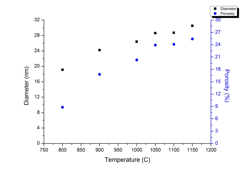
From the plot it can be seen that the porosity increases from 8.8% at 800C to 25.4% at 1150C. The pore diameter also increases from 19.1nm at 800C to 30.5nm at 1150C. One thing needs to be pointed out is the growth rate. Both the porosity and pore diameter increase quite fast with annealing temperature at beginning and seems to reach a plateau when the annealing temperature exceeds 1050C.
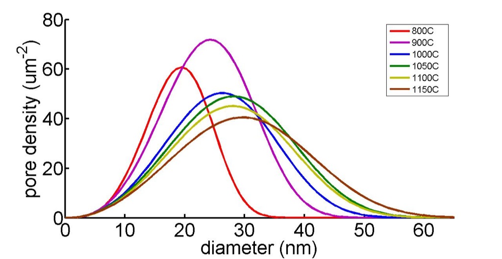
The next is the pore distribution plot. It shows the trend of pore distribution with annealing temperature. The pore size is relative small when the annealing temperature is below 1000C. That is why the distribution curve is somewhat narrow. When the annealing temperature increases, more and more bigger pores formed during the annealing and the pore distribution becomes broader as a result.
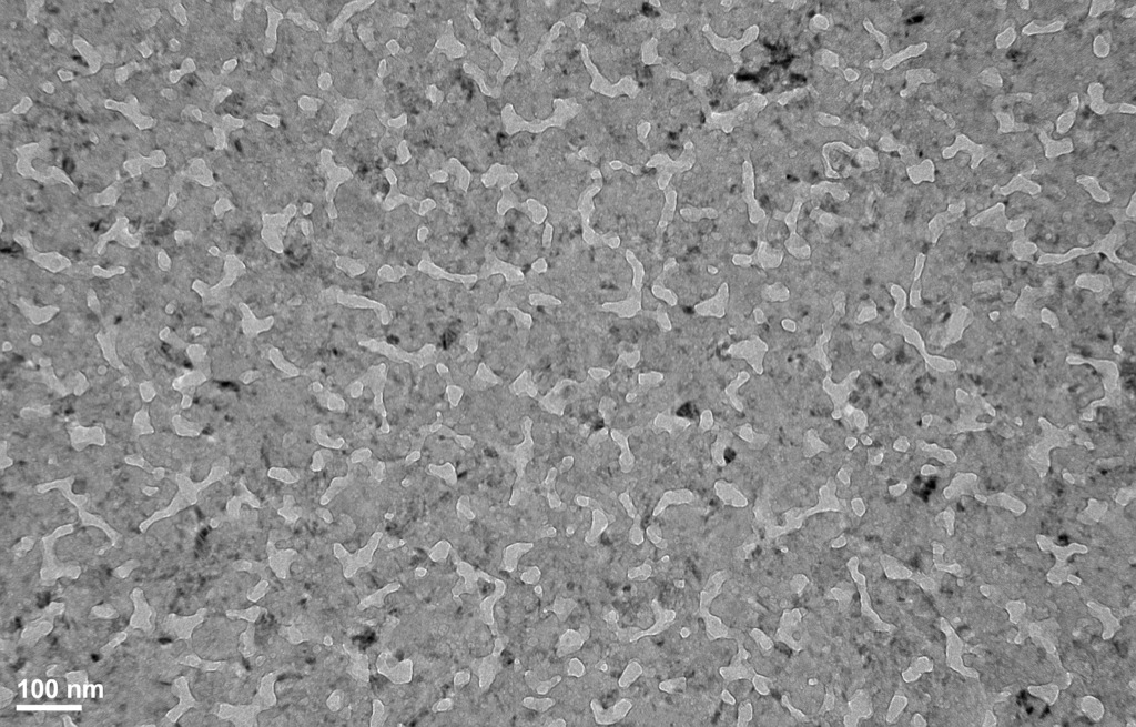
I also did a low temperature annealing at 700C. The following is an TEM image of the membrane. It can be seen that the shape of pores is quite irregular, more like a tear shape. The similar tear shape pores have also been observed in oxide/ silicon/ oxide stack at lower temperature annealing.
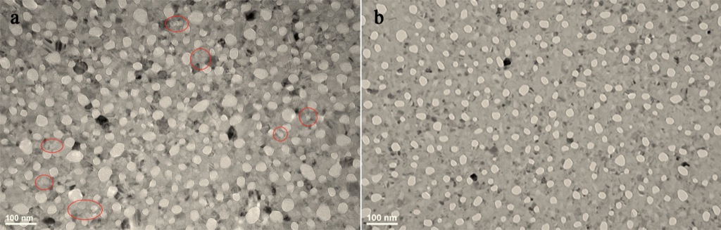
One interesting difference of pores between nitride/silicon/nitride system and oxide/silicon/oxide system is from the blind pores (non-through pores). The following are TEM images of pnc-Si membrane annealed at 1000C for 1 minute from nitride/silicon/nitride system (left) and oxide/silicon/oxide system (right). From the left image you can see that some non-through pores partially overlapped (circled area), which probably means different pits on both sides of the silicon membrane overlapped. It indicates that pits are first formed in both interfaces of silicon nitride-amorphous silicon but they don’t grow deeper to meet with each other to form through pores. This is different from the pores formed in oxide/silicon/oxide system, which seldom shows overlapped non-through pores.
In sum, this is the first time we show that pores can also be formed in nitride/silicon/nitride stack system. Bigger pores with high porosity pcn-Si membrane is achieved. The pore evolution with annealing temperature, which shows the pore size and porosity increase with annealing temperature, in nitride/silicon/nitride system behaves very similar as that of oxide/silicon/oxide system. It also proves that the thermal stress is not the key factor to drive pore formation. The initial stress and the interface may be the real mystery behind the pore formation.
The low temperature structures are interesting, but do we really think this is representative of the intermediate state of the membranes as it passes through these lower temperature to a higher annealing temperature.