SEM x-section of 30-50-30 NSN showing increased thickness after RTP
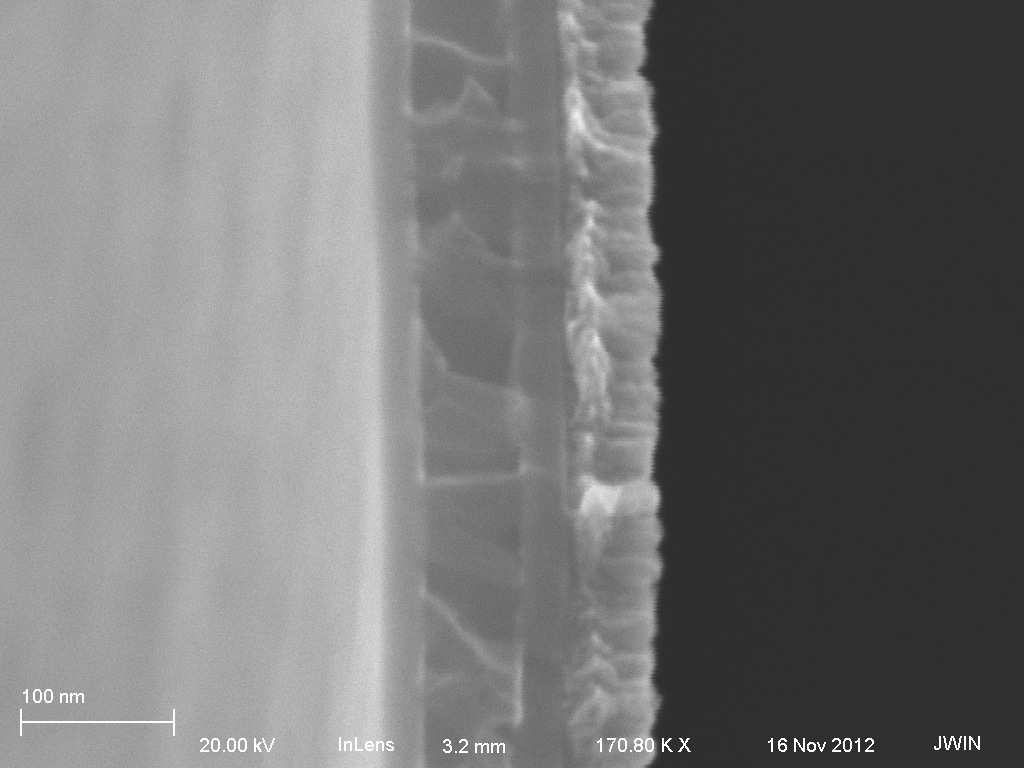
This is a continuation of earlier work showing 30-100-30 NSN x-sections where the Si layer thickness increases from ~92 nm before RTP to ~130 nm after RTP.
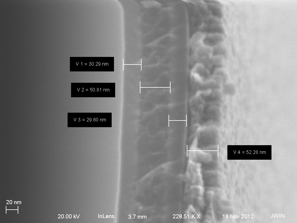
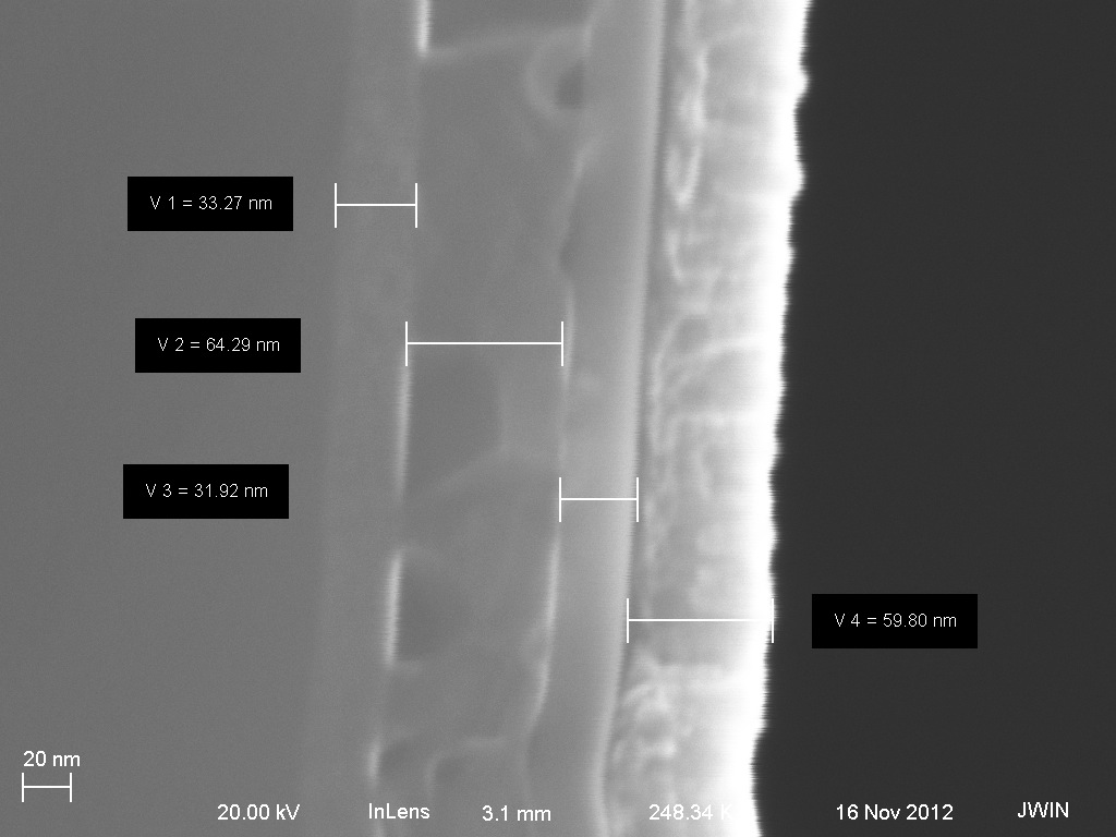
Below are SEMs showing a ~50 nm thick a-Si film becoming a ~62 nm thick pnc-Si. (1000 C, 50 C/s, 60 s in susceptor, RTP after EDP etch) I had a very difficult time imaging the samples as is, so I sputtered some Pt on top of some samples before cleaving them, hence the additional metal film on the stack.

can you quantify both the thickness increase and the porosity, and see if these 2 numbers are consistent? A quick calculation suggesst that the porosity should be 30% which is very high. This assumes no major strain state change of course…
For the 30-50-30 membrane the thickness increased from 50->62 nm indicating a porosity of 19 %. (assuming the density change from a-Si to nc-Si is insignificant) The measured porosity from TEM imaging is 17%.
The 30-100-30 membrane increased from 92->130 nm indicating a porosity of 29%. The porosity I measured from TEM was 10%.
I assume the difference in porosity numbers comes from the fact that porosity measured from the 2-dimensional TEM images does not correctly account for tortuous pores, pits, or enclosed void spaces.