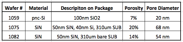
Burst Pressure: pnc-Si vs. NPN
This past year I have been collecting burst pressure data on pnc-Si and NPN. The data for 30nm pnc-Si came from my previous post, “Wafer 1059: Burst Pressure Analysis”, which also includes a wafer map. This wafer had 7% porosity and an average pore diameter of 20nm. I tested square window sizes with side lengths of 0.1mm, 0.3mm, 0.5mm, 0.7mm, and 0.9mm. Between 19 and 41 samples were tested for each window size.
Most recently, burst pressures for 50nm NPN were collected. First, I tested the same square window sizes as I did with pnc-Si. This wafer had 20% porosity and a 68nm average pore diameter. In addition, I burst chips from another wafer with side lengths of 0.3mm, 0.6mm, 0.9mm, 1.2mm, 1.5mm, and 1.8mm. This wafer had 14% porosity and a 54nm average pore diameter. Between 4 and 5 samples were tested for each NPN window size.
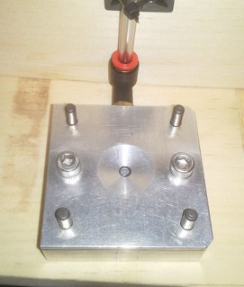
The burst pressure set up is shown below:
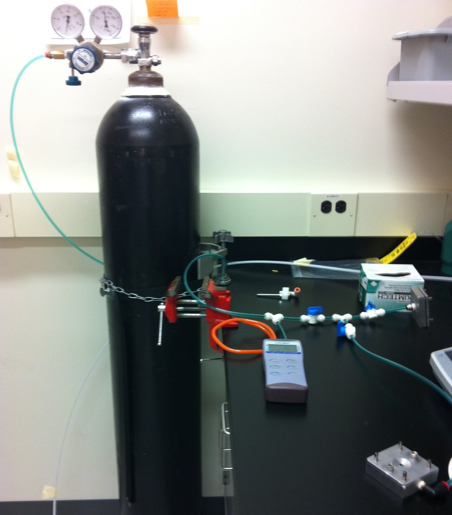
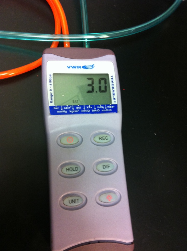
Max pressure is recorded using a manometer.
Three wafers were used in this experiment:
Below is a figure comparing burst pressure and square window area.

Below is a figure comparing burst pressure and square window side length.

In the above figures, I also included data for square window sizes with side lengths 0.1mm and 0.3mm from Mohammad’s chips. Here is the link to my previous post.
From examining these results, it is clear that SiN is stronger that pnc-Si. Deflection tests were performed on the two materials, and more is to come regarding this data. In addition, models explaining the trends observed in this data are under progress.