Variation of trans endothelial electrical resistance (TEER) with different membrane configurations
A bit of background: In order to quantify how permeable a tissue barrier is, we use a method known as trans epithelial electrical resistance (TEER). Cells are grown on a permeable growth substrate in a transwell format. When the cells are not confluent, there is a continuous diffusion of ions across the two sides of the membrane. This motion causes an electric current. As the cells grow more confluent, this motion gets hampered and we observe an increase in the resistance measurement as the time progresses. Thus resistance increase is a sign for confluency. In order to compare different systems with different growth area, we multiply the resistance value with the membrane area to obtain a normalized TEER value. Note that this area is the entire membrane area and not just a fraction of it that is porous in nature.
We always had troubles with TEER measurement, since our active area for 5 well sepcon is barely 1.5 mm2 as compared to the more commonly used 24 well format transwell, which has an active area of 33 mm2 i.e. 20 times more than ours. Thus even if we assemble our chip in this 24 well format transwell, our area-multiplication factor is so small that the TEER values usually are at least an order of magnitude lesser than the published ones. However it needs to be highlighted that the total cell growth area for a sepcon is 5.5*5.5 i.e. 30 mm2 with only 1.5 mm2 as the exposed area. So effectively what we have is a large density of pores concentrated in the center rather than having it uniformly spread over the entire membrane area (as in the case of commercial membranes). So what should be the ideal area multiplication factor: 1.5 mm2 or 30 mm2? In order to investigate this question in detail. I conducted following studies.
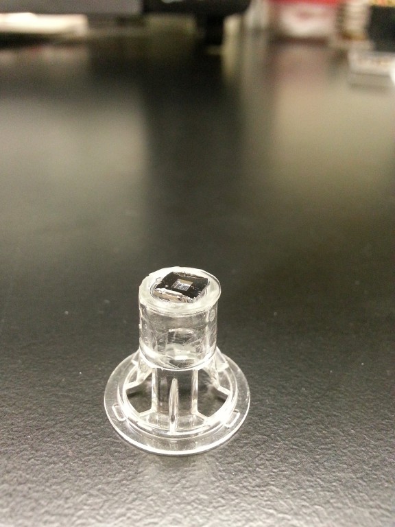
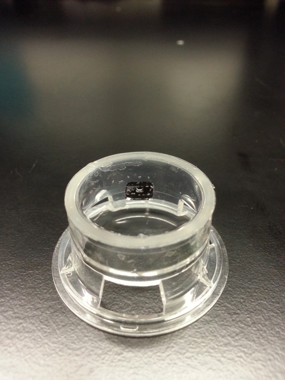
I took transwells of two different membrane sizes (33 mm2 and 467 mm2) and cut open the membrane from those wells and put our membrane on the top of those empty wells using silicone gaskets, as shown here.
Smaller bucket
Larger bucket
I took NPN membranes of 4 different window sizes from wafer 1082 from Sarah’s inventory: 0.9, 1.2, 1.5 and 1.8 mm, thus the areas are 0.81, 1.44, 2.25, 3.24 mm2
After assembly, I thus have 2 transwells with same active area but 2 different inactive areas, thus 8 wells in all.
I incubated 10x PBS on both sides of the wells in 70 degrees C for 1 hour, just to achieve diffusion equilibrium and steady state electrical behavior.
After 1 hour the TEER values are:
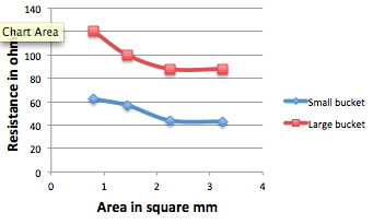
As expected the resistance decreases as the membrane active area increases. But what is the relation between different area systems? Looking at the product of resistance and active area:
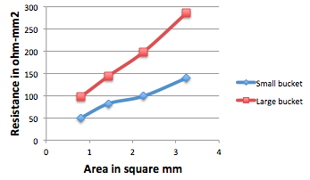
Thus normalizing the resistance by multiplying with the active area doesn’t seem to equalize the resistance values within different area systems. That is obvious from the first graph, since the resistance decreases linearly with area and not hyperbolically.
An interesting observation. When I increase the active are from 2.25 to 3.24 mm2 i.e. when I switch from 1.5 mm window size to 1.8 mm, I do not see any further drop in resistance. This probably indicates that with 2.25 mm2 of opening, we pretty much achieve a short circuit, and any further increase in the size of conductor is not going to alter the motion of charge carrier further. If we remove the last data point and fit a linear equation, we get these curves:
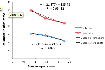
The essential difference between the small bucket and the large bucket is that, for same amount of active (window) area, there is an unequal amounts of inactive area. Also since the electrode sizes are same, the electric field is getting diffused more when there is more media as in the case of the larger bucket. This means that electric current density is less, but at the same time the number of charge carriers is more in the larger bucket. Somehow, our goal is to try to find a factor that relates the resistance in the systems with same total area (but different amounts of active area) to each other. At the same time, we must know how the resistance changes if we are keeping same active area, but changing inactive area. These pieces of information are important because all of our devices vary in geometry and may or may not have same active area. Hence a normalization factor is absolutely essential. Any thoughts? I am too confused!!!
I think your resistance values for the larger bucket may be directly related to the additional path length needed for the voltage drop from the edge of the larger bucket.
What we really want is our membranes to have 33 mm^2 active area, a direct analogue to the existing transwells. Since this would probably be difficult to use, we could create more windows on a larger chip, sampling the entire area, not just the center. I’m thinking like the nine windows of the TEM grid product. Then we could more rationally justify using the full cell growth area, not just the total window area.