Alternate Metal or Metal Oxide Nanomembranes
I have wondered if it were possible to create free-standing, nanoporous nanomembranes out of other materials (rather than my MgF2 process). The process is general enough that it should work. The major factors are
- Etch Selectivity between the substrate and the deposited material
- Film Mechanics (some films tear themselves apart due to the relative sizes and stresses inherent to the films)
- Coating Adhesion (can’t have a film if it doesn’t stick to itself and the substrate)
Based on the knowledge that it is difficult to create good dry etches for platinum and gold, I quickly threw a few membranes in the Denton sputter in the Wilmot SEM prep room.
Recipe
- 3x NPN substrates (Wafer 1024, 3-slots)
- Base pressure = 150 mTorr (Pt), 50 mTorr (Au)
- 3x Purge with Ar (300 mTorr), return to base pressure
- 6 nm/min @ 15 mA dep rate quoted (from tool instructions)
- Sputter Time = 300 seconds
- 10 second spike in sputter current for Au deposition (50 mA), recovered to 15 mA
- ideally produces 30 nm of film thickness

You can see the discoloration fairly easily on the gold-coated membranes, but not so much with the platinum ones.
I then used the SBT RIE in the south bay of URnano to remove the underlying silicon nitride. The tool was pumping down effectively, with base pressures in the single microtorr range. It had been a while since I had last run my process on the tool, so I wiped out the process chamber with IPA, then performed an Ar etch for 10 minutes, 100 W, 100 mTorr operating pressure.
Then, I proceeded to test my nitride etch recipe. I had very poor luck in times past trying to control the amount of oxygen in my plasma; the MFC was often unstable at the low volumes I asked of it. Previously, I compensated by increasing the pressure to stable amounts of oxygen, which increases the chances of polymer formation and other issues. This run of etches was fantastic by comparison; I was able to decrease the amount of oxygen and the operating etch pressure considerably.
Nitride Etch Recipe
- Non-operating
- CHF3 = 33 mTorr
- O2 = 2.5 mTorr
- Base Pressure = 1e-5 torr
- Gas Pressure = 40-45 mTorr
- Operating
- Pressure = 75 mTorr
- Power (Fwd/Rev) = 100/0 W
- Time = 90 s
- Ideally etches 40 nm/min (over etch is common to make sure all the silicon is gone)
I etched each chip separately with a companion NPN chip from Wafer 1024 to confirm the etch was working appropriately (4 runs). The variation run to run was very good (75-76 mtorr, 90 s, 100-103 W (0-2 W reflected)
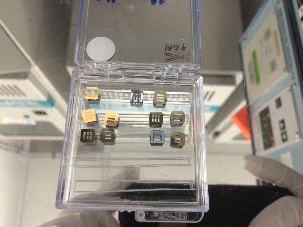


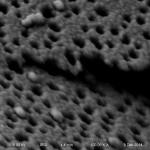
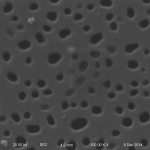
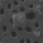
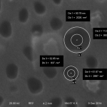
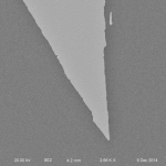
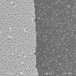
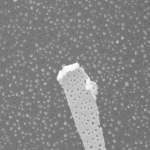
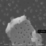
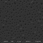
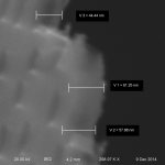
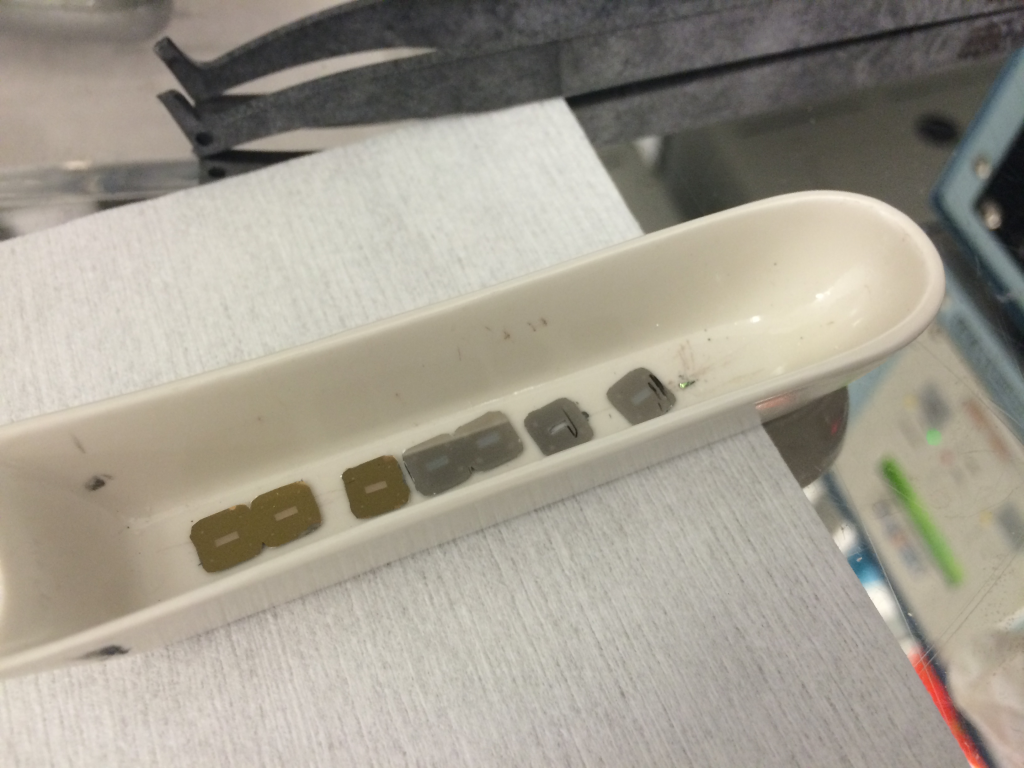
Here we have 3-slot gold nanomembranes that have probably been etched completely. I dropped one of the chips and it broke 2 of the windows (can be scratched with tweezers). The films look wrinkled under the scope. I will be confirming the results on the SEM later with EDAX to get the precise measurements of the deposited film purity, and regular SEM and STEM for thickness and porosity. The platinum film coating disintegrated under the same etch conditions.
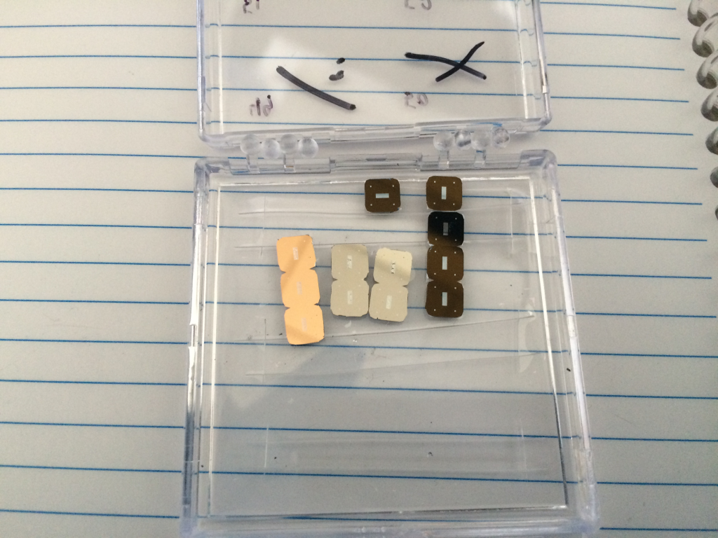
Gold Control (Au+NPN)

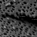
Gold Sample A (etched)
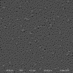
Gold Sample B (etched)
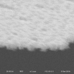
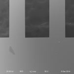
Platinum Control (Pt + NPN)
With the above information in mind, I could probably have annealed the platinum coating at 450 C for 2 hrs in an Ar ambient (1 sL/min) to make them stronger before etching (like my MgF2 process). I threw in a few gold-coated nanomembranes as well to see what it would do to the films, but they did not survive the etching process. The same recipe was used as above to coat the nanomembranes, but this time, I used chips from wafer 1153 (NPN, 35 nm, 15%). After etching 2 chips, one large nanomembrane survived the process, but the vias all survived.
I similarly did an interesting thing with ITO. I deposited 25 nm of ITO onto 5 chips from wafer 1153 at 175 C using the Lesker sputter system in the cleanroom. The recipe I used was “ITO Deposition – 250 A”. Electrically, the freshly deposited material measured 2.35 kohms across the width of a glass coverslip, and 3 kohms across the length. Upon observation, the films appeared to be heavily wrinkled, and the 2 chips I used did not survive the etching process. I annealed the remaining 3 films at 450 C for 2 hrs in an Ar environment (1-1.2 sL/min) which changed the film color substantially. When I etched, none of the large membranes survived the process, but some of the vias survived.

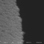
How can we use nanoporous alternative material nanomembranes? It has been suggested to us by a recent visitor that the structure would have some very interesting plasmonic effects. After some research, however, there doesn’t usually need to be a need for high purity nanomembranes; removing the silicon is not particularly necessary (a notable counterexample is my work with Kevin, where the actual measurement is hindered by silicon). We could potentially turn these structures into electrodes for energy storage, due to their increased surface area, using the nanostructured portion as a seed for nanotube growth. Alternatively, there may be other materials that could work well here (palladium for nanomembrane-catalysts). All in all, it shows that we are able to create porous thin films out of some different kinds of materials other than silicon.
Very cool! Anxious to see pores. Probably not that critical to have all the nitride removed in this case, right?